JAJSSX0B January 2022 – January 2024 TPS61376
PRODUCTION DATA
- 1
- 1 特長
- 2 アプリケーション
- 3 概要
- 4 Pin Configuration and Functions
- 5 Specifications
-
6 Detailed Description
- 6.1 Overview
- 6.2 Functional Block Diagram
- 6.3
Feature Description
- 6.3.1 VCC Power Supply
- 6.3.2 Enable and Programmable UVLO
- 6.3.3 Soft Start and Inrush Current Control During Start-Up
- 6.3.4 Switching Frequency
- 6.3.5 Adjustable input average Current Limit
- 6.3.6 Shut Down and Load Disconnect
- 6.3.7 Overvoltage Protection
- 6.3.8 Output Short Protection
- 6.3.9 Thermal Shutdown
- 6.4 Device Functional Modes
- 7 Application and Implementation
- 8 Device and Documentation Support
- 9 Revision History
- 10Mechanical, Packaging, and Orderable Information
7.2.2.7 Loop Stability
The TPS61376 requires external compensation, which allows the loop response to be optimized for each application. The COMP pin is the output of the internal error amplifier. An external compensation network, comprised of resistor RC, and ceramic capacitors CC and CP, is connected to the COMP pin.
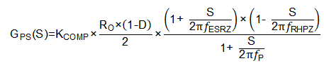
The power stage small signal loop response of constant off-time (COT) with peak current control can be modeled by Equation 12.
where
- D is the switching duty cycle.
- RO is the output load resistance.
- KCOMP is power stage trans-conductance (inductor peak current / comp voltage), which is 6.5A/V.
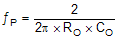
where
- CO is effective output capacitance.
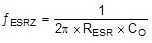
where
- RESR is the equivalent series resistance of the output capacitor.
The COMP pin is the output of the internal transconductance amplifier. Equation 16 shows the small signal transfer function of compensation network.
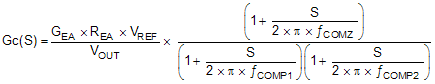
where
- GEA is the transconductance of the amplifier, which is 240uS.
- REA is the output resistance of the amplifier, which is 100MΩ.
- VREF is the reference voltage at the FB pin.
- VOUT is the output voltage.
- ƒCOMP1, ƒCOMP2 are the frequency of the poles of the compensation network.
- ƒCOMZ is the zero's frequency of the compensation network.
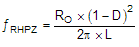
The next step is to choose the loop crossover frequency, ƒC. The higher frequency that the loop gain stays above zero before crossing over, the faster the loop response is. It is generally accepted that the loop gain cross over no higher than the lower of either 1/10 of the switching frequency, ƒSW, or 1/5 of the RHPZ frequency, ƒRHPZ.
Then set the value of RC, CC, and CP (in Figure 7-1) by following these equations.
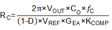
where
- ƒC is the selected crossover frequency.
The value of CC can be set by Equation 18.

The value of CP can be set by Equation 19.
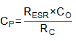
If the calculated value of CP is less than 10pF, it can be left open.
Designing the loop for greater than 45° of phase margin and greater than 10dB gain margin eliminates output voltage ringing during the line and load transient.