SLVSC68A June 2015 – June 2015 TPS62745 , TPS627451
PRODUCTION DATA.
- 1 Features
- 2 Applications
- 3 Description
- 4 Typical Application Schematic
- 5 Device Comparison Table
- 6 Pin Configuration and Functions
- 7 Specifications
- 8 Detailed Description
- 9 Application and Implementation
- 10Power Supply Recommendations
- 11Layout
- 12Device and Documentation Support
- 13Mechanical, Packaging, and Orderable Information
パッケージ・オプション
メカニカル・データ(パッケージ|ピン)
- DSS|12
サーマルパッド・メカニカル・データ
- DSS|12
発注情報
1 Features
- Input Voltage Range VIN from 3.3 V to 10 V
- Typical 400 nA Quiescent Current
- Up to 90% efficiency with load currents >15 µA
- Up to 300 mA Output Current
- RF Friendly DCS-Control™
- Low Output Ripple Voltage
- 16 Selectable Output Voltages from
- 1.8 V to 3.3 V (TPS62745)
- 1.3 V to 2.8 V (TPS627451)
- Integrated input voltage switch
- Integrated Discharge Function at VOUT
- Open Drain Power Good Output
- Operates with a Tiny 3.3 µH or 4.7 µH Inductor
- Small 3 mm x 2 mm WSON Package
2 Applications
- Bluetooth® Low Energy, RF4CE, Zigbee
- Industrial Metering
- Energy Harvesting
3 Description
The TPS62745 is a high efficiency ultra low power synchronous step down converter optimized for low power wireless applications. It provides a regulated output voltage consuming only 400-nA quiescent current. The device operates from two rechargeable Li-Ion batteries, Li-primary battery chemistries such as Li-SOCl2, Li-SO2, Li-MnO2 or four to six cell alkaline batteries. The input voltage range up to 10 V allows also operation from a USB port and thin-film solar modules. The output voltage is set with four VSEL pins between 1.8 V and 3.3 V for TPS62745 or 1.3 V and 2.8 V for TPS627451. TPS62745 features low output ripple voltage and low noise with a small output capacitor. An internal input voltage switch controlled by pin EN_VIN_SW connects the supply voltage to pin VIN_SW. The switch is intended to be used for an external voltage divider, scaling down the input voltage for an external ADC. The switch is automatically opened when the supply voltage is below the undervoltage lockout threshold. The TPS62745 is available in a small 12 pin 3 mm × 2 mm WSON package.
Device Information(1)
| PART NUMBER | PACKAGE | BODY SIZE (NOM) |
|---|---|---|
| TPS62745 | WSON | 3 mm x 2 mm |
| TPS627451 |
- For all available packages, see the orderable addendum at the end of the datasheet.
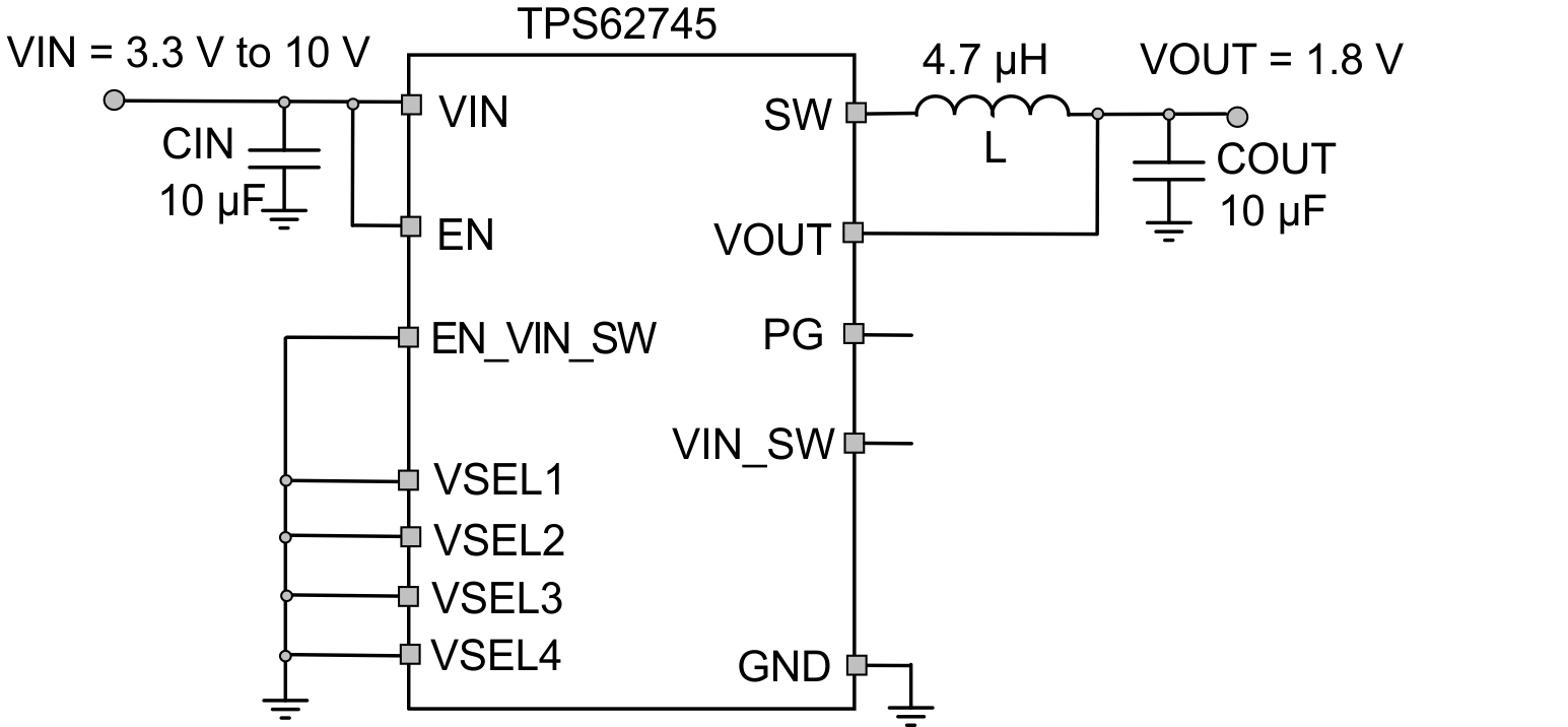
4 Typical Application Schematic
spacer
spacer

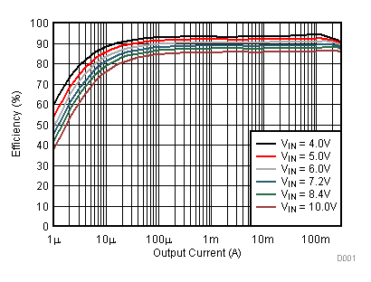
Efficiency vs Output Current; Vo = 3.3 V
