JAJSNG4B January 2015 – January 2022 TPS65251-1 , TPS65251-2 , TPS65251-3
PRODUCTION DATA
- 1 特長
- 2 アプリケーション
- 3 概要
- 4 Revision History
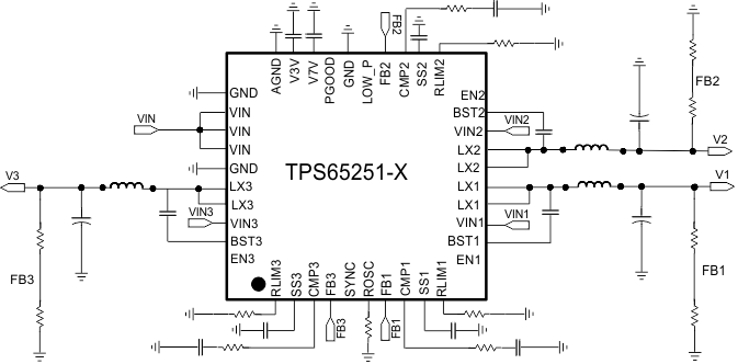
- 5 Pin Configuration and Functions
- 6 Specifications
-
7 Detailed Description
- 7.1 Overview
- 7.2 Functional Block Diagram
- 7.3
Feature Description
- 7.3.1 Adjustable Switching Frequency
- 7.3.2 Synchronization
- 7.3.3 Out-of-Phase Operation
- 7.3.4 Delayed Start-Up
- 7.3.5 Soft-Start Time
- 7.3.6 Adjusting the Output Voltage
- 7.3.7 Input Capacitor
- 7.3.8 Bootstrap Capacitor
- 7.3.9 Error Amplifier
- 7.3.10 Slope Compensation
- 7.3.11 Power Good
- 7.3.12 3.3-V and 6.5-V LDO Regulators
- 7.3.13 Current Limit Protection
- 7.3.14 Overvoltage Transient Protection (OVP)
- 7.3.15 Thermal Shutdown
- 7.4 Device Functional Modes
-
8 Application and Implementation
- 8.1 Application Information
- 8.2
Typical Application
- 8.2.1 Design Requirements
- 8.2.2
Detailed Design Procedure
- 8.2.2.1 Loop Compensation Circuit
- 8.2.2.2 Selecting the Switching Frequency
- 8.2.2.3 Output Inductor Selection
- 8.2.2.4 Output Capacitor
- 8.2.2.5 Input Capacitor
- 8.2.2.6 Soft-Start Capacitor
- 8.2.2.7 Bootstrap Capacitor Selection
- 8.2.2.8 Adjustable Current Limiting Resistor Selection
- 8.2.2.9 Output Voltage and Feedback Resistors Selection
- 8.2.2.10 Compensation
- 8.2.2.11 3.3-V and 6.5-V LDO Regulators
- 8.2.3 Application Curves
- 9 Power Supply Recommendations
- 10Layout
- 11Device and Documentation Support
- 12Mechanical, Packaging, and Orderable Information
パッケージ・オプション
メカニカル・データ(パッケージ|ピン)
- RHA|40
サーマルパッド・メカニカル・データ
- RHA|40
発注情報
3 概要
TPS65251-x には、入力電圧範囲が広く高効率の同期整流降圧コンバータが 3個搭載されています。これらのコンバータは、アプリケーションを簡素化するとともに、対象アプリケーションに応じて使用方法を最適化できるように設計されています。
コンバータは、5、9、12、15Vのシステムで動作し、パワー・トランジスタが内蔵されています。出力電圧は外付けの分圧抵抗を使用して、0.8V から入力電源電圧近くまでの任意の値に設定できます。各コンバータにはイネーブル・ピンがあり、シーケンシングの目的で遅延スタートアップが可能です。ソフトスタート・ピンでソフトスタート・コンデンサを選択することによりソフトスタート時間を変更でき、電流制限 (RLIMx) ピンで外付け抵抗を選択するとともに最適なインダクタを選択して、電流制限を設定できます。電流モード制御によって、RC補償が簡単になります。
コンバータのスイッチング周波数は、ROSC ピンに接続される外付け抵抗で設定するか、または必要に応じて SYNC ピンに接続される外部クロックに同期させることもできます。スイッチング・レギュレータは、300kHz~2.2MHz で動作するように設計されています。降圧 1 と降圧 2、3 は 180° の位相差で動作するため (降圧 2 と 降圧 3 は同相動作)、入力フィルタの要件が最小限になります。
TPS65251-x にはスーパバイザ回路があり、各コンバータの出力を監視します。シーケンシングが完了し、すべてのPG信号が通知され、選択可能なリセット終了時間が経過すると、PGOOD ピンがアサートされます。PGOOD 信号の極性は、アクティブ HIGH です。
すべてのコンバータには自動の低消費電力パルス PFM スキップ・モードが搭載されているため、軽負荷やスタンバイ動作時の効率が向上し、同時に非常に小さな出力リップルが保証され、低い出力電圧で 2% 未満という値を実現できます。
| 部品番号 | パッケージ(1) | 本体サイズ (公称) |
|---|---|---|
| TPS65251-1 | VQFN (40) | 6.00mm × 6.00mm |
| TPS65251-2 | ||
| TPS65251-3 |