JAJSNG4B January 2015 – January 2022 TPS65251-1 , TPS65251-2 , TPS65251-3
PRODUCTION DATA
- 1 特長
- 2 アプリケーション
- 3 概要
- 4 Revision History
- 5 Pin Configuration and Functions
- 6 Specifications
-
7 Detailed Description
- 7.1 Overview
- 7.2 Functional Block Diagram
- 7.3
Feature Description
- 7.3.1 Adjustable Switching Frequency
- 7.3.2 Synchronization
- 7.3.3 Out-of-Phase Operation
- 7.3.4 Delayed Start-Up
- 7.3.5 Soft-Start Time
- 7.3.6 Adjusting the Output Voltage
- 7.3.7 Input Capacitor
- 7.3.8 Bootstrap Capacitor
- 7.3.9 Error Amplifier
- 7.3.10 Slope Compensation
- 7.3.11 Power Good
- 7.3.12 3.3-V and 6.5-V LDO Regulators
- 7.3.13 Current Limit Protection
- 7.3.14 Overvoltage Transient Protection (OVP)
- 7.3.15 Thermal Shutdown
- 7.4 Device Functional Modes
-
8 Application and Implementation
- 8.1 Application Information
- 8.2
Typical Application
- 8.2.1 Design Requirements
- 8.2.2
Detailed Design Procedure
- 8.2.2.1 Loop Compensation Circuit
- 8.2.2.2 Selecting the Switching Frequency
- 8.2.2.3 Output Inductor Selection
- 8.2.2.4 Output Capacitor
- 8.2.2.5 Input Capacitor
- 8.2.2.6 Soft-Start Capacitor
- 8.2.2.7 Bootstrap Capacitor Selection
- 8.2.2.8 Adjustable Current Limiting Resistor Selection
- 8.2.2.9 Output Voltage and Feedback Resistors Selection
- 8.2.2.10 Compensation
- 8.2.2.11 3.3-V and 6.5-V LDO Regulators
- 8.2.3 Application Curves
- 9 Power Supply Recommendations
- 10Layout
- 11Device and Documentation Support
- 12Mechanical, Packaging, and Orderable Information
パッケージ・オプション
メカニカル・データ(パッケージ|ピン)
- RHA|40
サーマルパッド・メカニカル・データ
- RHA|40
発注情報
8.2.3 Application Curves
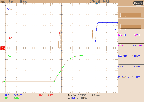 Figure 8-3 Buck 1 Start-Up (Ch3 = VIN)
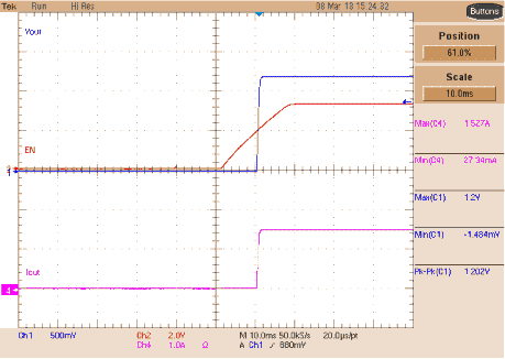 Figure 8-5 Buck 1 Start-Up 1.5-A Resistive
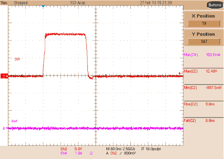 Figure 8-7 Buck 1 Switching Node, No Load
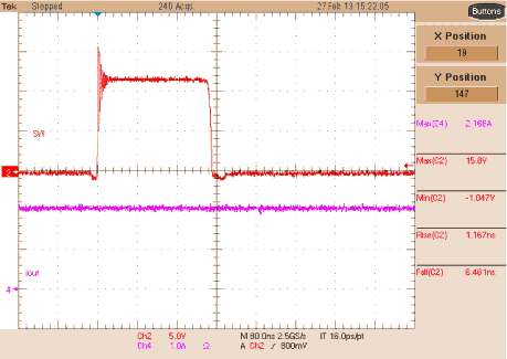 Figure 8-9 Buck 1 Switching Node, 2-A Load
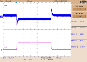 Figure 8-11 Buck 1 Dynamic Response, 0- to 1-A Step
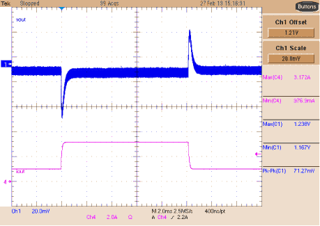 Figure 8-13 Buck 1 Dynamic Response, 1-A to 3-A Step
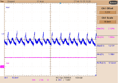 Figure 8-15 Buck 1 Ripple, 2-A Load
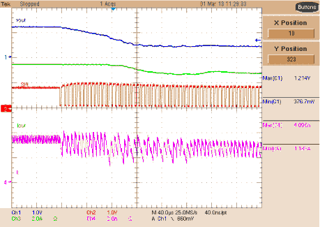
| Ch1 = VOUT | Ch2 = COMP1 | Ch3 = IOUT |
| Ch4 = Inductor |
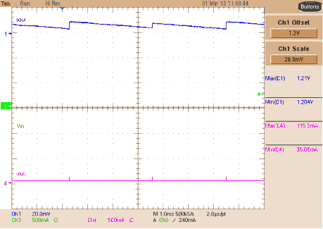 Figure 8-19 Buck 1 Low-Power Output, No Load
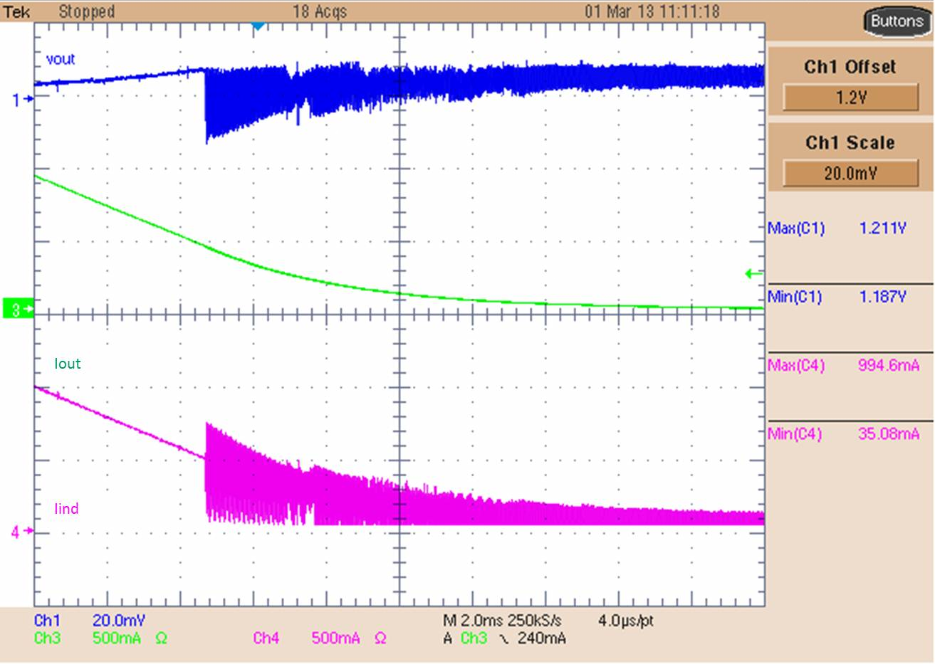
| Ch1 = VOUT | Ch3 = IOUT | Ch4 = Inductor |

| Ch3 = VIN | ||
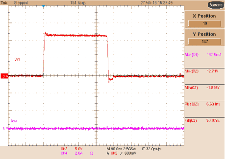 Figure 8-25 Buck 2 Switching Node, No Load
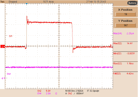 Figure 8-27 Buck 2 Switching Node, 2-A Load
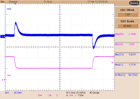 Figure 8-29 Buck 2 Dynamic Response, 1-A to 2-A Step
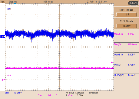 Figure 8-31 Buck 2 Ripple, 1-A Load
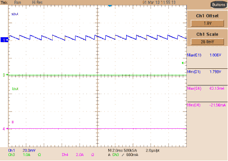 Figure 8-33 Buck 2 Low-Power Output, No Load
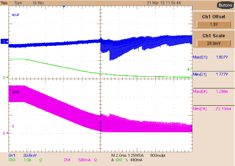
| Ch1 = VOUT | Ch3 = IOUT | Ch4 = Inductor |
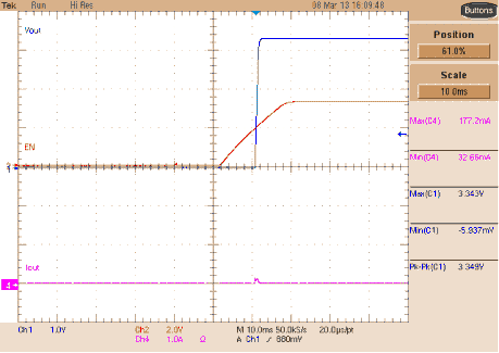
| Ch3 = VIN | ||
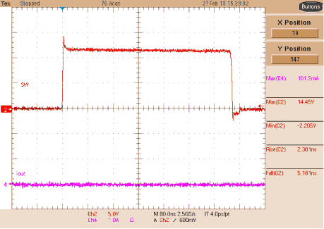 Figure 8-39 Buck 3 Switching Node, No Load
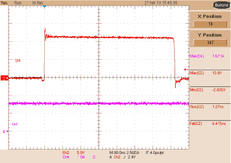 Figure 8-41 Buck 3 Switching Node, 1.5-A Load
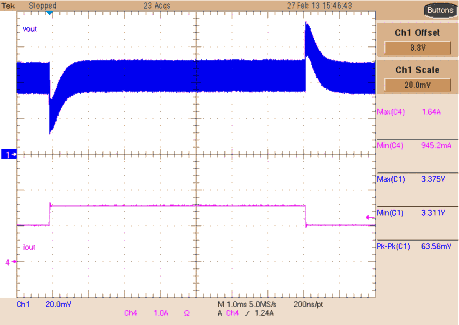 Figure 8-43 Buck 3 Dynamic Response, 1-A to 1.5-A Step
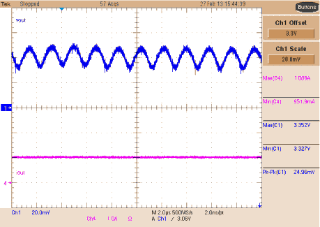 Figure 8-45 Buck 3 Ripple, 1-A Load
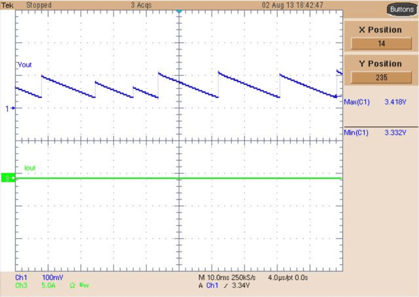 Figure 8-47 Buck 3 Low-Power Output, No Load
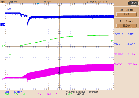
| Ch1 = VOUT | Ch3 = IOUT | Ch4 = Inductor |
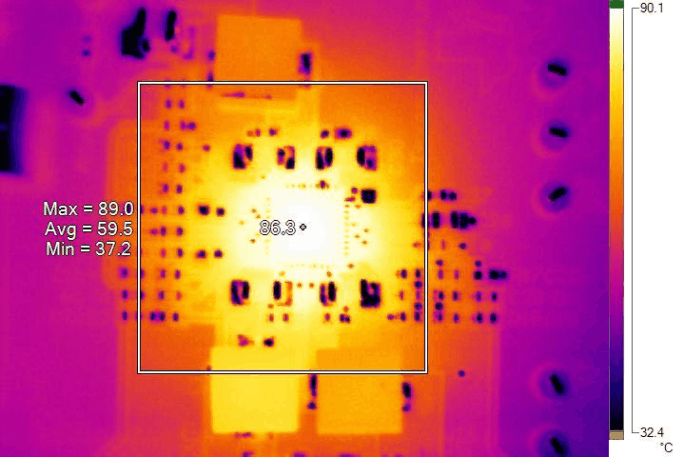 Figure 8-51 Temperature Profile, VO = 1.2 V, IO = 3 A, VO = 1.8 V, IO = 2 A, VO = 3.3 V, IO = 2 A, TA = 28°C
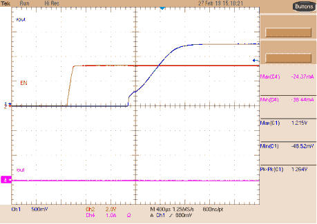 Figure 8-4 Buck 1 Soft-Start
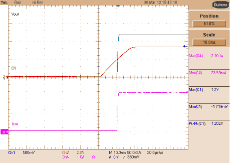 Figure 8-6 Buck 1 Soft-Start 2-A Load
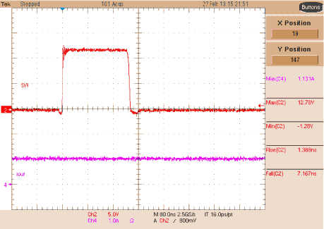 Figure 8-8 Buck 1 Switching Node, 1-A Load
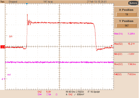 Figure 8-10 Buck 1 Switching Node, 3-A Load
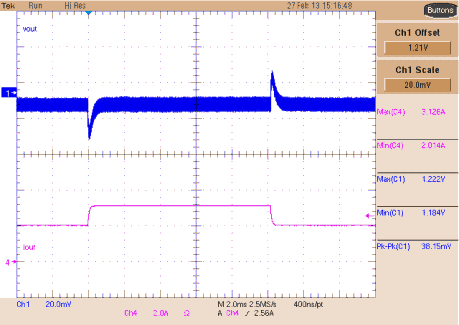 Figure 8-12 Buck 1 Dynamic Response, 2-A to 3-A Step
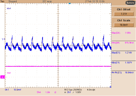 Figure 8-14 Buck 1 Ripple, 1-A Load
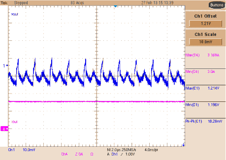 Figure 8-16 Buck 1 Ripple, 3-A Load
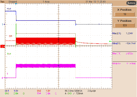
| Ch1 = VOUT | Ch2 = COMP1 | Ch3 = IOUT |
| Ch4 = Inductor |
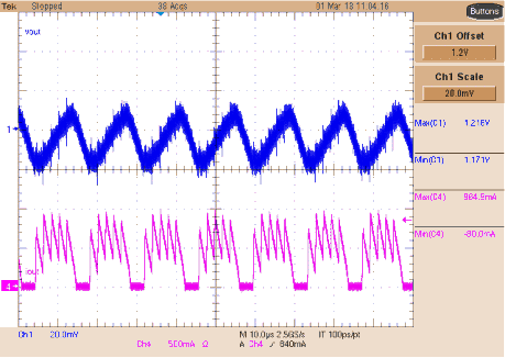 Figure 8-20 Buck 1 Low-Power Operation
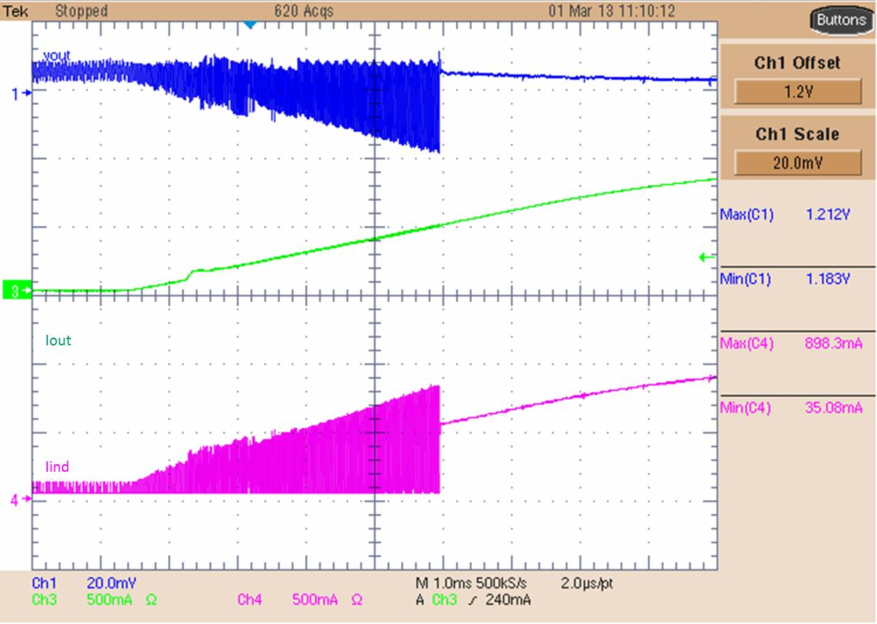
| Ch1 = VOUT | Ch3 = IOUT | Ch4 = Inductor |
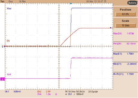 Figure 8-24 Buck 2 Start-Up, 2-A Load
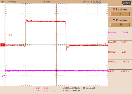 Figure 8-26 Buck 2 Switching Node, 1-A Load
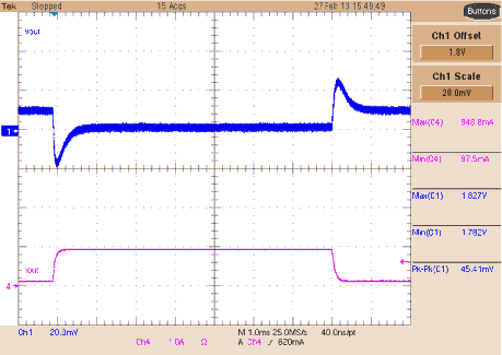 Figure 8-28 Buck 2 Dynamic Response, 0-A to 1-A Step
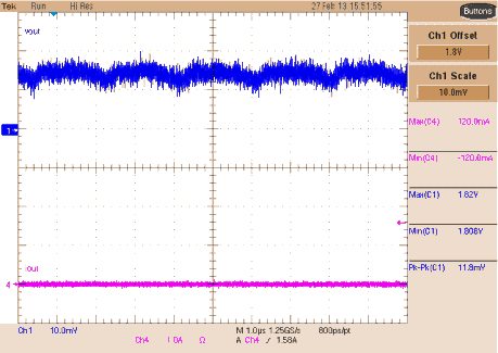 Figure 8-30 Buck 2 Ripple, No Load
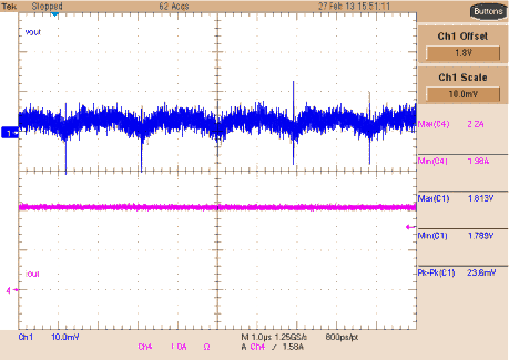 Figure 8-32 Buck 2 Ripple, 3-A Load
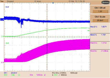
| Ch1 = VOUT | Ch3 = IOUT | Ch4 = Inductor |
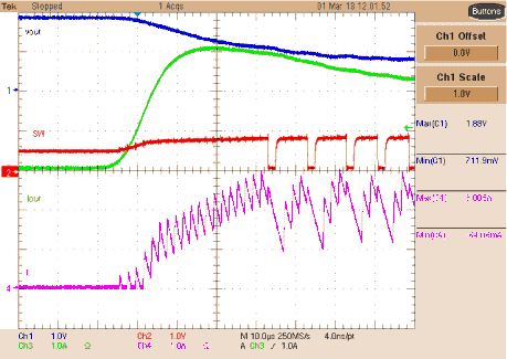
| Ch1 = VOUT | Ch2 = COMP1 | Ch3 = IOUT |
| Ch4 = Inductor |
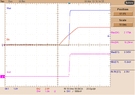 Figure 8-38 Buck 3 Soft-Start
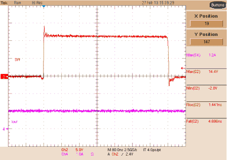 Figure 8-40 Buck 3 Switching Node, 1-A Load
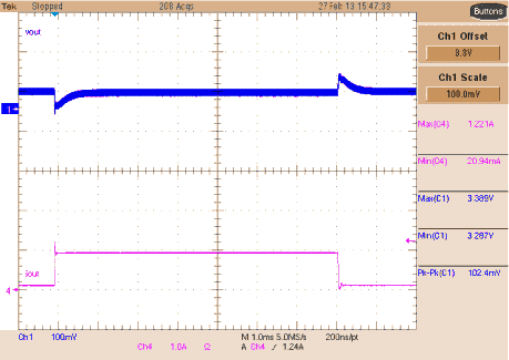 Figure 8-42 Buck 3 Dynamic Response, 0-A to 1-A Step
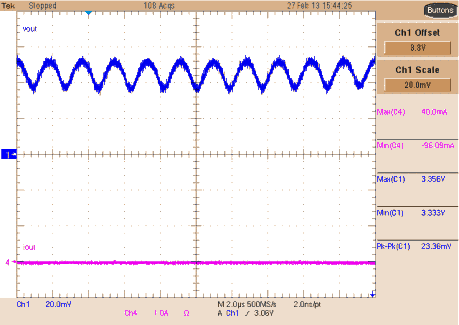 Figure 8-44 Buck 3 Ripple, No Load
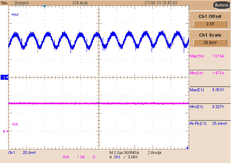 Figure 8-46 Buck 3 Ripple, 3-A Load
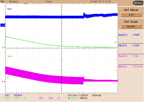
| Ch1 = VOUT | Ch3 = IOUT | Ch4 = Inductor |
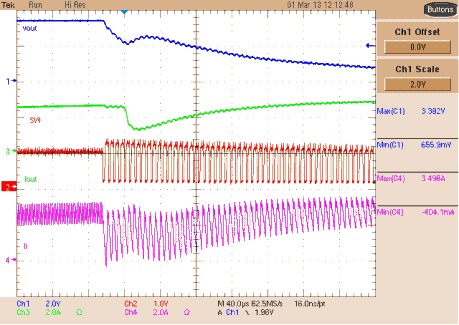
| Ch1 = VOUT | Ch2 = COMP1 | Ch3 = IOUT |
| Ch4 = Inductor |