JAJSNG4B January 2015 – January 2022 TPS65251-1 , TPS65251-2 , TPS65251-3
PRODUCTION DATA
- 1 特長
- 2 アプリケーション
- 3 概要
- 4 Revision History
- 5 Pin Configuration and Functions
- 6 Specifications
-
7 Detailed Description
- 7.1 Overview
- 7.2 Functional Block Diagram
- 7.3
Feature Description
- 7.3.1 Adjustable Switching Frequency
- 7.3.2 Synchronization
- 7.3.3 Out-of-Phase Operation
- 7.3.4 Delayed Start-Up
- 7.3.5 Soft-Start Time
- 7.3.6 Adjusting the Output Voltage
- 7.3.7 Input Capacitor
- 7.3.8 Bootstrap Capacitor
- 7.3.9 Error Amplifier
- 7.3.10 Slope Compensation
- 7.3.11 Power Good
- 7.3.12 3.3-V and 6.5-V LDO Regulators
- 7.3.13 Current Limit Protection
- 7.3.14 Overvoltage Transient Protection (OVP)
- 7.3.15 Thermal Shutdown
- 7.4 Device Functional Modes
-
8 Application and Implementation
- 8.1 Application Information
- 8.2
Typical Application
- 8.2.1 Design Requirements
- 8.2.2
Detailed Design Procedure
- 8.2.2.1 Loop Compensation Circuit
- 8.2.2.2 Selecting the Switching Frequency
- 8.2.2.3 Output Inductor Selection
- 8.2.2.4 Output Capacitor
- 8.2.2.5 Input Capacitor
- 8.2.2.6 Soft-Start Capacitor
- 8.2.2.7 Bootstrap Capacitor Selection
- 8.2.2.8 Adjustable Current Limiting Resistor Selection
- 8.2.2.9 Output Voltage and Feedback Resistors Selection
- 8.2.2.10 Compensation
- 8.2.2.11 3.3-V and 6.5-V LDO Regulators
- 8.2.3 Application Curves
- 9 Power Supply Recommendations
- 10Layout
- 11Device and Documentation Support
- 12Mechanical, Packaging, and Orderable Information
パッケージ・オプション
メカニカル・データ(パッケージ|ピン)
- RHA|40
サーマルパッド・メカニカル・データ
- RHA|40
発注情報
7.4.1 Low-Power/Pulse Skipping Operation
When a synchronous buck converter operates at light load or standby conditions, the switching losses are the dominant source of power losses. Under these load conditions, TPS65251-x uses a pulse skipping modulation technique to reduce the switching losses by keeping the power transistors in the off-state for several switching cycles, while maintaining a regulated output voltage. Figure 7-4 shows the output voltage and load plus the inductor current.
 Figure 7-4 Low Power/Pulse Skipping
During the burst mode, the converter continuously charges up the output capacitor until the output voltage reaches a certain limit threshold. The operation of the converter in this interval is equivalent to the peak inductor current mode control. In each switch period, the main switch is turned on until the inductor current reaches the peak current limit threshold. As the load increases, the number of pulses increases to make sure that the output voltage stays within regulation limits. When the load is very light, the low-power controller has a zero crossing detector to allow the low-side MOSFET to operate even in light load conditions. The transistor is not disabled at light loads. A zero crossing detection circuit disables it when inductor current reverses. During the whole process, the body diode does not conduct, but is used as blocking diode only.
During the skipping interval, the upper and lower transistors are turned off and the converter stays in idle mode. The output capacitors are discharged by the load current until the moment when the output voltage drops to a low threshold.
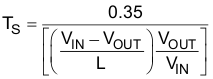
The choice of output filter influences the performance of the low-power circuit. The maximum ripple during low-power mode can be calculated as:
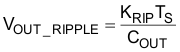
where
- KRIP is 1.4 for Buck 1.
- KRIP is 0.7 for Buck 2 and Buck 3.
TS can be calculated as: