JAJSC12D October 2013 – April 2018
PRODUCTION DATA.
- 1 特長
- 2 アプリケーション
- 3 概要
- 4 改訂履歴
- 5 概要(続き)
- 6 Device Comparison
- 7 Pin Configuration and Functions
- 8 Specifications
- 9 Detailed Description
- 10Application and Implementation
- 11Power Supply Recommendations
- 12Layout
- 13デバイスおよびドキュメントのサポート
- 14メカニカル、パッケージ、および注文情報
パッケージ・オプション
メカニカル・データ(パッケージ|ピン)
- PWP|20
サーマルパッド・メカニカル・データ
- PWP|20
発注情報
11.1.1 LDO Dropout Recovery Explained
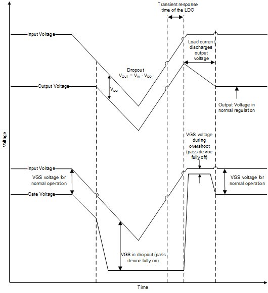
When an LDO is in dropout the output voltage is below the accuracy specification. This condition causes the error amplifier to force the gate of the pass transistor such that the pass transistor is fully on and provides the least resistance possible, meaning VOUT tracks VIN as closely as possible. When the input voltage recovers, the error amplifier must force the gate of the pass device to the opposite rail making the pass transistor more resistive. The change in gate voltage takes a finite amount of time, as dictated by the bandwidth of the error amplifier. If VIN rises quickly during that time then VOUT tracks VIN and overshoots above the nominal output voltage. Figure 25 depicts a graphical representation of an LDO recovering from dropout.
The amplitude of the overshoot is determined by both the speed of the VIN ramp and the transient response of the LDO, which determines how long is required for the error amplifier to respond to changes on VOUT. The amount of time required for the overshoot to be discharged is determined by the load current that must drain the excess charge that has accumulated on COUT.
 Figure 25. LDO Response Entering and Exiting Dropout