SLVSCJ8B November 2014 – January 2015
PRODUCTION DATA.
- 1 Features
- 2 Applications
- 3 Description
- 4 Typical Application Schematic
- 5 Revision History
- 6 Pin Configuration and Functions
- 7 Specifications
- 8 Detailed Description
- 9 Application and Implementation
- 10Power Supply Recommendations
- 11Layout
- 12Device and Documentation Support
- 13Mechanical, Packaging, and Orderable Information
パッケージ・オプション
メカニカル・データ(パッケージ|ピン)
サーマルパッド・メカニカル・データ
- DCY|4
発注情報
9 Application and Implementation
NOTE
Information in the following applications sections is not part of the TI component specification, and TI does not warrant its accuracy or completeness. TI’s customers are responsible for determining suitability of components for their purposes. Customers should validate and test their design implementation to confirm system functionality.
9.1 Application Information
The TPS7B69xx-Q1 family of devices is a 150-mA low-dropout linear regulator designed for up to 40-V VI operation with only 15-µA quiescent current at light loads. Use the PSpice transient model to evaluate the base function of the device. To download the PSpice transient model, go to the device product folder on www.TI.com. In addition to this model, specific evaluation modules (EVM) are available for these devices. For the EVM and the EVM user guide, go to the device product folder.
9.2 Typical Application
Figure 25 shows the typical application circuit for the TPS7B69xx-Q1 family of devices. Based on the end-application, different values of external components can be used. An application can require a larger output capacitor during fast load steps to achieve better load transient response. TI recommends a low-ESR ceramic capacitor with a dielectric of type X5R or X7R for better load transient response.
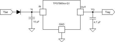 Figure 25. Typical Application Schematic for TPS7B69xx-Q1
9.2.1 Design Requirements
For this design example, use the parameters listed in Table 1.
Table 1. Design Parameters
| DESIGN PARAMETER | EXAMPLE VALUES |
|---|---|
| Input voltage range | 4 to 40 V |
| Output voltage | 2.5 V, 3.3 V, 5 V |
| Output current rating | 150 mA |
| Output capacitor range | 2.2 to 100 µF |
| Output capacitor ESR range | 1 mΩ to 2 Ω |
9.2.2 Detailed Design Procedure
To begin the design process, determine the following:
- Input voltage range
- Output Voltage
- Output current rating
9.2.2.1 Input Capacitor
The device requires an input decoupling capacitor, the value of which depends on the application. The typical recommend value for the decoupling capacitor is higher than 0.1 µF. The voltage rating must be greater than the maximum input voltage.
9.2.2.2 Output Capacitor
The device requires an output capacitor to stabilize the output voltage. The output capacitor value should be between 2.2 µF and 100 µF. The ESR value range should be between 1 mΩ and 2 Ω. TI recommends a ceramic capacitor with low ESR to improve the load transient response.
9.2.2.3 Power Dissipation and Thermal Considerations
Use Equation 1 to calculate the power dissipated in the device.
where
- PD = continuous power dissipation
- IO = output current
- VI = input voltage
- VO = output voltage
Because IQ « IO, the term IQ × VI in Equation 1 can be ignored.
For a device under operation at a given ambient air temperature (TA), use Equation 2 to calculate the junction temperature (TJ).
where
- ZθJA = junction-to-ambient air thermal impedance
Use Equation 3 to calculate the rise in junction temperature because of power dissipation.
For a given maximum junction temperature (TJmax), use Equation 4 to calculate the maximum ambient air temperature (TAmax) at which the device can operate.
9.2.3 Application Curve
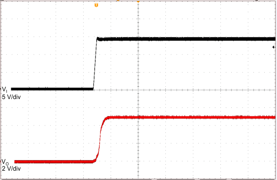
| CO = 2.2 µF, 400 µs/div |