SLVSCJ8B November   2014  – January 2015

PRODUCTION DATA.  

  1. Features
  2. Applications
  3. Description
  4. Typical Application Schematic
  5. Revision History
  6. Pin Configuration and Functions
  7. Specifications
    1. 7.1 Absolute Maximum Ratings
    2. 7.2 ESD Ratings
    3. 7.3 Recommended Operating Conditions
    4. 7.4 Thermal Information
    5. 7.5 Electrical Characteristics
    6. 7.6 Typical Characteristics
  8. Detailed Description
    1. 8.1 Overview
    2. 8.2 Functional Block Diagram
    3. 8.3 Feature Description
      1. 8.3.1 Input (IN)
      2. 8.3.2 Output (OUT)
      3. 8.3.3 Output Capacitor Selection
      4. 8.3.4 Low-Voltage Tracking
      5. 8.3.5 Thermal Shutdown
    4. 8.4 Device Functional Modes
      1. 8.4.1 Operation With VI Less Than 4 V
      2. 8.4.2 Operation With VI Greater Than 4 V
  9. Application and Implementation
    1. 9.1 Application Information
    2. 9.2 Typical Application
      1. 9.2.1 Design Requirements
      2. 9.2.2 Detailed Design Procedure
        1. 9.2.2.1 Input Capacitor
        2. 9.2.2.2 Output Capacitor
        3. 9.2.2.3 Power Dissipation and Thermal Considerations
      3. 9.2.3 Application Curve
  10. 10Power Supply Recommendations
  11. 11Layout
    1. 11.1 Layout Guidelines
    2. 11.2 Layout Example
  12. 12Device and Documentation Support
    1. 12.1 Documentation Support
      1. 12.1.1 Related Documentation
    2. 12.2 Related Links
    3. 12.3 Trademarks
    4. 12.4 Electrostatic Discharge Caution
    5. 12.5 Glossary
  13. 13Mechanical, Packaging, and Orderable Information

パッケージ・オプション

メカニカル・データ(パッケージ|ピン)
サーマルパッド・メカニカル・データ
発注情報

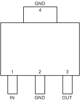
6 Pin Configuration and Functions

DCY Package
4-Pin SOT-223
Top View
po_dcy_slvscj8.gif
DBV Package
5-Pin SOT-23
Top View
po_dbv_slvscj8.gif
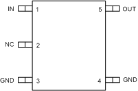
NC - No internal connection

Pin Functions

PIN TYPE DESCRIPTION
NAME NO.
SOT-223 SOT-23
GND 2 3 G Ground reference
4 4
IN 1 1 P Input power-supply voltage
NC 2 Not connected pin
OUT 3 5 P Output voltage