SLVSCJ8B November 2014 – January 2015
PRODUCTION DATA.
- 1 Features
- 2 Applications
- 3 Description
- 4 Typical Application Schematic
- 5 Revision History
- 6 Pin Configuration and Functions
- 7 Specifications
- 8 Detailed Description
- 9 Application and Implementation
- 10Power Supply Recommendations
- 11Layout
- 12Device and Documentation Support
- 13Mechanical, Packaging, and Orderable Information
パッケージ・オプション
メカニカル・データ(パッケージ|ピン)
サーマルパッド・メカニカル・データ
- DCY|4
発注情報
11 Layout
11.1 Layout Guidelines
For the layout of TPS7B69xx-Q1 family of devices, place the input and output capacitors close to the devices as shown in Figure 27 and Figure 28. To enhance the thermal performance, TI recommends surrounding the device with some vias.
Minimize equivalent series inductance (ESL) and ESR to maximize performance and ensure stability. Place every capacitor as close as possible to the device and on the same side of the PCB as the regulator.
Do not place any of the capacitors on the opposite side of the PCB from where the regulator is installed. TI strongly discourages the use of long traces because they can impact system performance negatively and even cause instability.
If possible, and to ensure the maximum performance specified in this product data sheet, use the same layout pattern used for the TPS7B69xx-Q1 evaluation board.
11.2 Layout Example
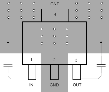 Figure 27. Layout Example for SOT-223 Package
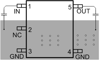 Figure 28. Layout Example for SOT-23 Package