SLUSBU2A September 2014 – February 2016 TPS92661-Q1
PRODUCTION DATA.
- 1 Features
- 2 Applications
- 3 Description
- 4 Revision History
- 5 Pin Configuration and Functions
- 6 Specifications
-
7 Detailed Description
- 7.1 Overview
- 7.2 Functional Block Diagram
- 7.3
Feature Description
- 7.3.1 Controlling the Internal LED Bypass Switches
- 7.3.2 Internal Switch Resistance
- 7.3.3 PWM Dimming
- 7.3.4 PWM Clock
- 7.3.5 PWM Synchronization
- 7.3.6 Switch Slew Control
- 7.3.7 Effect of Phase Shifting LED Duty Cycles
- 7.3.8 LED Fault Detection and Protection
- 7.3.9 Glitch-Free Operation
- 7.3.10 Internal Oscillator and Watchdog Timers
- 7.4
Device Functional Modes
- 7.4.1
Digital Interface Connections
- 7.4.1.1 Address (ADR0, ADR1, and ADR2 Pins)
- 7.4.1.2 Clock (CLK Pin)
- 7.4.1.3 Internal Charge Pump (CPP Pin)
- 7.4.1.4 Enable (EN Pin)
- 7.4.1.5 GND Pin
- 7.4.1.6 Receive (RX Pin)
- 7.4.1.7 Synchronization (SYNC Pin)
- 7.4.1.8 Transmit (TX Pin)
- 7.4.1.9 Primary Power Supply (VIN Pin)
- 7.4.1.10 On-Board 3.3-V Supply (VCC Pin)
- 7.4.2 Internal Pin-to-Pin Resistance
- 7.4.3 UART Physical Layer
- 7.4.4 UART Clock and Baudrate
- 7.4.5 UART Communications Reset
- 7.4.6 UART Device Addressing
- 7.4.7 UART Communications Protocol
- 7.4.8 Transaction Frame Description
- 7.4.9 Frame Initialization Byte
- 7.4.10 Register Address
- 7.4.11 Data Bytes
- 7.4.12 CRC Bytes
- 7.4.13 Registers
- 7.4.1
Digital Interface Connections
- 7.5 Programming
- 7.6 Register Map
- 8 Application and Implementation
- 9 Power Supply Recommendations
- 10Layout
- 11Device and Documentation Support
- 12Mechanical, Packaging, and Orderable Information
パッケージ・オプション
メカニカル・データ(パッケージ|ピン)
- PHP|48
サーマルパッド・メカニカル・データ
- PHP|48
発注情報
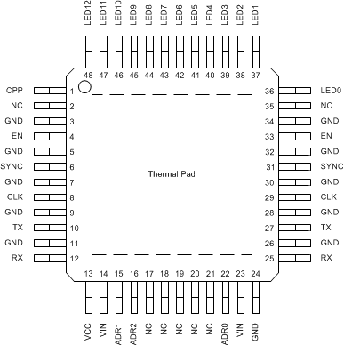
5 Pin Configuration and Functions
PHP Package
48-Pin TQFP
Top View

Pin Functions
| PIN | I/O | DESCRIPTION | |
|---|---|---|---|
| NAME | NO. | ||
| ADR0 | 22 | I | Least significant bit (LSB) of device address. Connect to VIN or GND. |
| ADR1 | 15 | I | Second bit of device address. Connect to VIN or GND. |
| ADR2 | 16 | I | Most significant bit (MSB) of device address. Connect to VIN or GND. |
| CLK | 8 | I | System clock. This clock is provided externally (by the microcontroller unit or an external oscillator) and is the primary clock for the device. |
| 29 | |||
| CPP | 1 | I | Charge pump output. Bypass with a ceramic capacitor with a minimum value of 0.1 µF to LED12. |
| EN | 4 | I | Enable pins. The device is active when EN is high or in reset when EN is low. Connect to microcontroller unit output or tie to VCC or VIN for enable at power-up. |
| 33 | |||
| GND | 3, 5, 7, 9, 11, 24, 26, 28, 30, 32, 34 | — | Device system ground. All pins MUST be connected for proper operation. |
| LED0 | 36 | O | Connect to cathode of LED1. |
| LED1 | 37 | O | Connect to anode of LED1 and cathode of LED2. |
| LED2 | 38 | O | Connect to anode of LED2 and cathode of LED3. |
| LED3 | 39 | O | Connect to anode of LED3 and cathode of LED4. |
| LED4 | 40 | O | Connect to anode of LED4 and cathode of LED5. |
| LED5 | 41 | O | Connect to anode of LED5 and cathode of LED6. |
| LED6 | 42 | O | Connect to anode of LED6 and cathode of LED7. |
| LED7 | 43 | O | Connect to anode of LED7 and cathode of LED8. |
| LED8 | 44 | O | Connect to anode of LED8 and cathode of LED9. |
| LED9 | 45 | O | Connect to anode of LED9 and cathode of LED10. |
| LED10 | 46 | O | Connect to anode of LED10 and cathode of LED11. |
| LED11 | 47 | O | Connect to anode of LED11 and cathode of LED12. |
| LED12 | 48 | O | Connect to anode of LED12. |
| NC | 2, 17, 18, 19, 20, 21, 35 | — | No connection. |
| RX | 12 | I/O | Received data pins. Connect one RX pin of first device to microcontroller unit TX output and use second pin to connect to a RX pin of the second device. All other devices use both pins to route the RX line through each device. |
| 25 | |||
| SYNC | 6 | I/O | Synchronization pins. Allows synchronization of multiple TPS92661 devices on the same network. May be driven by the microcontroller unit, or one TPS92661 device may be programmed via the serial interface to provide this pulse. Only one device should drive this signal. May be left unconnected if not used. |
| 31 | |||
| TX | 10 | I/O | Transmitted data pins. Connect one TX pin of first device to microcontroller unit RX input and use second pin to connect to a TX pin of the second device. All other devices use both pins to route the TX line through each device. This pin requires a 100kΩ pull-up resistor. |
| 27 | |||
| VCC | 13 | O | Output of the on-board 3.3-V LDO. This pin requires a ceramic output capacitor with a value of 0.1 µF or greater. Tie to the VIN pin for 5-V microcontroller unit systems. |
| VIN | 14 | I | 5-V power supply input for device. Bypass with a ceramic capacitor with a minimum value of 0.1 µF. |
| 23 | |||
| Thermal Pad | - | Connect to system GND. | |