JAJSN59 April 2022 TPSM63603E
PRODUCTION DATA
- 1 特長
- 2 アプリケーション
- 3 概要
- 4 Revision History
- 5 Device Comparison Table
- 6 Pin Configuration and Functions
-
7 Specifications
- 7.1 Absolute Maximum Ratings
- 7.2 ESD Ratings
- 7.3 Recommended Operating Conditions
- 7.4 Thermal Information
- 7.5 Electrical Characteristics
- 7.6 System Characteristics
- 7.7 Typical Characteristics
- 7.8 Typical Characteristics — VIN = 12 V
- 7.9 Typical Characteristics — VIN = 24 V
- 7.10 Typical Characteristics — VIN = 36 V
-
8 Detailed Description
- 8.1 Overview
- 8.2 Functional Block Diagram
- 8.3
Feature Description
- 8.3.1 Input Voltage Range
- 8.3.2 Adjustable Output Voltage (FB)
- 8.3.3 Input Capacitors
- 8.3.4 Output Capacitors
- 8.3.5 Switching Frequency (RT)
- 8.3.6 Output ON and OFF Enable (EN/SYNC) and VIN UVLO
- 8.3.7 Frequency Synchronization (EN/SYNC)
- 8.3.8 Spread Spectrum
- 8.3.9 Power-Good Monitor (PG)
- 8.3.10 Adjustable Switch-Node Slew Rate (RBOOT and CBOOT)
- 8.3.11 Internal LDO, VCC Output, and VLDOIN Input
- 8.3.12 Overcurrent Protection (OCP)
- 8.3.13 Thermal Shutdown
- 8.4 Device Functional Modes
-
9 Applications and Implementation
- 9.1 Application Information
- 9.2 Typical Applications
- 10Power Supply Recommendations
- 11Layout
- 12Device and Documentation Support
- 13Mechanical, Packaging, and Orderable Information
8.3.3 Input Capacitors
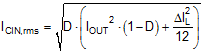
Input capacitors are required to limit the input ripple voltage to the module due to switching-frequency AC currents. TI recommends using ceramic capacitors to provide low impedance and high RMS current rating over a wide temperature range. Equation 2 gives the input capacitor RMS current. The highest input capacitor RMS current occurs at D = 0.5, at which point, the RMS current rating of the capacitors must be greater than half the output current.
where
- D = VOUT / VIN is the module duty cycle.
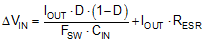
Ideally, the DC and AC components of the input current to the buck stage are provided by the input voltage source and the input capacitors, respectively. Neglecting inductor ripple current, the input capacitors source current of amplitude (IOUT – IIN) during the D interval and sink IIN during the 1 – D interval. Thus, the input capacitors conduct a square-wave current of peak-to-peak amplitude equal to the output current. The resulting capacitive component of the AC ripple voltage is a triangular waveform. Together with the ESR-related ripple component, Equation 3 gives the peak-to-peak ripple voltage amplitude.
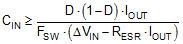
Equation 4 gives the input capacitance required for a particular load current.
where
- ΔVIN is the input voltage ripple specification.
The TPSM63603E requires a minimum of 2 × 4.7-µF ceramic type input capacitance. Only use high-quality ceramic type capacitors with sufficient voltage and temperature rating. The ceramic input capacitors provide a low impedance source to the converter in addition to supplying the ripple current and isolating switching noise from other circuits. Additional capacitance can be required for applications with transient load requirements. The voltage rating of the input capacitors must be greater than the maximum input voltage. To compensate for the derating of ceramic capacitors, TI recommends a voltage rating of twice the maximum input voltage or placing multiple capacitors in parallel. Table 8-2 includes a preferred list of capacitors by vendor.
| Vendor(1) | Dielectric | Part Number | Case Size | Capacitor Characteristics | |
|---|---|---|---|---|---|
| Voltage Rating (V) | Capacitance (µF)(2) | ||||
| TDK | X7R | C3216X7R1H475K160AC | 1206 | 50 | 4.7 |
| Murata | X7R | GRM31CR71H475KA12L | 1206 | 50 | 4.7 |
| TDK | X7R | CGA6P3X7R1H475K250AB | 1210 | 50 | 4.7 |
| Murata | X7S | GCM31CC71H475KA03L | 1206 | 50 | 4.7 |