SCDS358B November 2014 – February 2015 TS3A227E
PRODUCTION DATA.
- 1 Features
- 2 Applications
- 3 Description
- 4 Simplified Schematic
- 5 Revision History
- 6 Pin Configuration and Functions
- 7 Specifications
- 8 Parameter Measurement Information
-
9 Detailed Description
- 9.1 Overview
- 9.2 Functional Block Diagram
- 9.3 Feature Description
- 9.4 Device Functional Modes
- 9.5 Register Maps
- 9.6
Register Field Descriptions
- 9.6.1 Device ID Register Field Descriptions (Address 00h)
- 9.6.2 Interrupt Register Field Descriptions (Address 01h)
- 9.6.3 Key Press Interrupt Register Field Descriptions (Address 02h)
- 9.6.4 Interrupt Disable Register Field Descriptions (Address 03h)
- 9.6.5 Device Settings Field Descriptions (Address 04h)
- 9.6.6 Key Press Settings 1 Field Descriptions (Address 05h)
- 9.6.7 Key Press Settings 2 Field Descriptions (Address 06h)
- 9.6.8 Switch Control 1 Field Descriptions (Address 07h)
- 9.6.9 Switch Control 2 Field Descriptions (Address 08h)
- 9.6.10 Switch Status 1 Field Descriptions (Address 09h)
- 9.6.11 Switch Status 2 Field Descriptions (Address 0Ah)
- 9.6.12 Detection Results Field Descriptions (Address 0Bh)
- 9.6.13 ADC Output Field Descriptions (Address 0Ch)
- 9.6.14 Threshold 1 Field Descriptions (Address 0Dh)
- 9.6.15 Threshold 2 Field Descriptions (Address 0Eh)
- 9.6.16 Threshold 3 Field Descriptions (Address 0Fh)
- 10Application and Implementation
- 11Power Supply Recommendations
- 12Layout
- 13Device and Documentation Support
- 14Mechanical, Packaging, and Orderable Information
パッケージ・オプション
メカニカル・データ(パッケージ|ピン)
サーマルパッド・メカニカル・データ
- RVA|16
発注情報
6 Pin Configuration and Functions
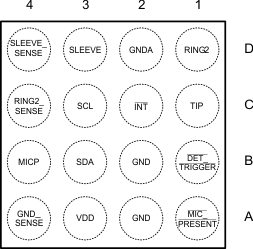
DSBGA – YFF
Top View
QFN – RVA
Top View
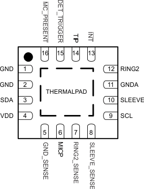
Pin Functions
| PIN | TYPE | DESCRIPTION | ||
|---|---|---|---|---|
| NAME | RVA | YFF | ||
| DET_TRIGGER | 15 | B1 | I/O | A falling edge from high to low on this pin triggers accessory detection. This pin can be connected the headset jack to allow automatic pull-down to ground after headset insertion to initialize detection. |
| GND | 1, 2 | A2, B2 | GND | Primary ground connection for the TS3A227E. Must be connected to system ground. |
| GNDA | 11 | D2 | I/O | Ground connection for the internal ground FETs of the TS3A227E. If FM is being supported connect this pin to the FM matching network. If FM is not being support connect this pin to system ground. |
| GND_SENSE | 5 | A4 | I/O | Ground sense line for the codec. |
| INT | 13 | C2 | GND | Open drain interrupt output from the TS3A227E to notify the host that an event has occurred. If I2C is not used this pin must be grounded. |
| MIC_PRESENT | 16 | A1 | I/O | Open drain output to indicate to the host that a headset with a microphone is inserted.. |
| MICP | 6 | B4 | I/O | Microphone signal connection to the codec. Microphone bias is applied to this pin. |
| RING2 | 12 | D1 | O | Headset current return path if RING2 is ground for the headset. Connect to 3.5 mm jack RING2 connection with low DC resistance trace. |
| RING2_SENSE | 7 | C4 | GND | Connected to the RING2 pin of the 3.5 mm jack. If RING2 pin on plug in is MIC signal, this is connected to MICP. If not, this is connected to GND_SENSE and becomes the ground sensing feedback for the accessory |
| SCL | 9 | C3 | I | Clock from I2C bus. This can be connected to VDD if I2C is not used. |
| SDA | 3 | B3 | I/O | Bidirectional data from/to I2C bus. This can be connected to VDD if I2C is not used. |
| SLEEVE | 10 | D3 | O | Headset current return path if SLEEVE is GND for headset. Connect to 3.5 mm jack SLEEVE connection with low DC resistance trace. |
| SLEEVE_SENSE | 8 | D4 | GND | Connected to the SLEEVE pin of the 3.5 mm jack. If SLEEVE pin on plug in is MIC signal, this is connected to MICP. If not, this is connected to GND_SENSE and becomes the ground sensing feedback for the accessory |
| THERMAL PAD | GND | The THERMAL PAD of the RVA – QFN package must be connected to any internal PCB ground plane using multiple vias for best thermal performance. | ||
| TIP | 14 | C1 | I/O | Connect to the TIP pin of the 3.5 mm jack. |
| VDD | 4 | A3 | PWR | Power input to the TS3A227E. External de-coupling capacitors are required on this pin. |