SCDS358B November 2014 – February 2015 TS3A227E
PRODUCTION DATA.
- 1 Features
- 2 Applications
- 3 Description
- 4 Simplified Schematic
- 5 Revision History
- 6 Pin Configuration and Functions
- 7 Specifications
- 8 Parameter Measurement Information
-
9 Detailed Description
- 9.1 Overview
- 9.2 Functional Block Diagram
- 9.3 Feature Description
- 9.4 Device Functional Modes
- 9.5 Register Maps
- 9.6
Register Field Descriptions
- 9.6.1 Device ID Register Field Descriptions (Address 00h)
- 9.6.2 Interrupt Register Field Descriptions (Address 01h)
- 9.6.3 Key Press Interrupt Register Field Descriptions (Address 02h)
- 9.6.4 Interrupt Disable Register Field Descriptions (Address 03h)
- 9.6.5 Device Settings Field Descriptions (Address 04h)
- 9.6.6 Key Press Settings 1 Field Descriptions (Address 05h)
- 9.6.7 Key Press Settings 2 Field Descriptions (Address 06h)
- 9.6.8 Switch Control 1 Field Descriptions (Address 07h)
- 9.6.9 Switch Control 2 Field Descriptions (Address 08h)
- 9.6.10 Switch Status 1 Field Descriptions (Address 09h)
- 9.6.11 Switch Status 2 Field Descriptions (Address 0Ah)
- 9.6.12 Detection Results Field Descriptions (Address 0Bh)
- 9.6.13 ADC Output Field Descriptions (Address 0Ch)
- 9.6.14 Threshold 1 Field Descriptions (Address 0Dh)
- 9.6.15 Threshold 2 Field Descriptions (Address 0Eh)
- 9.6.16 Threshold 3 Field Descriptions (Address 0Fh)
- 10Application and Implementation
- 11Power Supply Recommendations
- 12Layout
- 13Device and Documentation Support
- 14Mechanical, Packaging, and Orderable Information
パッケージ・オプション
メカニカル・データ(パッケージ|ピン)
サーマルパッド・メカニカル・データ
発注情報
7 Specifications
7.1 Absolute Maximum Ratings
over operating free-air temperature range referenced with respect to GND (unless otherwise noted)(1)| MIN | MAX | UNIT | ||
|---|---|---|---|---|
| Input Voltage | VDD | –0.3 | 5 | V |
| SDA, SCL, INT, MIC_PRESENT | –0.3 | VDD + 0.5 | V | |
| TIP | –3.3 | VDD + 0.5 | V | |
| DET_TRIGGER | –2.2 | VDD + 0.5 | V | |
| GND_SENSE, RING2, SLEEVE, RING2_SENSE, SLEEVE_SENSE, MICP, GNDA | –0.3 | 3.6(2) and VDD + 0.5 | V | |
| ON-state switch current | Combined continuous current through R2GNDFET and SLV GNDFET | 500 | mA | |
| Continuous current through R2DFET and SLV DFET | 50 | |||
| Continuous current through S1 | 20 | |||
| Continuous current through S2 | 20 | |||
| Continuous current through S3PR | 50 | |||
| Continuous current through S3PS | 50 | |||
| Continuous current through S3GR | 100 | |||
| Continuous current through S3GS | 100 | |||
| Operating ambient temperature range | –40 | 85 | °C | |
| Tstg | Storage temperature range | –65 | 150 | °C |
(1) Stresses beyond those listed under Absolute Maximum Ratings may cause permanent damage to the device. These are stress ratings only, which do not imply functional operation of the device at these or any other conditions beyond those indicated under Recommended Operating Conditions. Exposure to absolute-maximum-rated conditions for extended periods may affect device reliability.
(2) This rating is exclusive and the voltage on the pins must not exceed either 3.6 and VDD. E.g. if VDD = 4.5 V the voltage on the pin must not exceed 3.6 V and if VDD is = 2.5 V the voltage on the pin must not exceed 3.0 V.
7.2 ESD Ratings
| VALUE | UNIT | |||
|---|---|---|---|---|
| V(ESD) | Electrostatic discharge | Human body model (HBM), ESD stress voltagenew note #1 to the ESD Ratings table and combined MIN MAX column to VALUE (1)(2) | ±2000 | V |
| Charged device model (CDM), ESD stress voltage(1)(3) | ±500 | V | ||
| Contact discharge model (IEC) ESD stress voltage on TIP, DET_TRIGGER, RING2_SENSE, SLEEVE_SENSE, RING2, SLEEVE(1) | ±8000 | V | ||
(1) Electrostatic Discharge (ESD) to measure device sensitivity and immunity to damage caused by assembly line electrostatic discharges into the device
(2) JEDEC document JEP155 states that 500-V HBM allows safe manufacturing with a standard ESD control process.
(3) JEDEC document JEP157 states that 250-V CDM allows safe manufacturing with a standard ESD control process.
7.3 Recommended Operating Conditions
over operating free-air temperature range (unless otherwise noted)| MIN | MAX | UNIT | |||
|---|---|---|---|---|---|
| VDD | Power supply voltage range | 2.5 | 4.5 | V | |
| VI | Digital input voltage range | SDA, SCL | 0 | VDD | V |
| DET_TRIGGER | –2.2 | VDD | V | ||
| VIO | Input/output voltage range | RING2_SENSE, SLEEVE_SENSE, RING2, SLEEVE, GND_SENSE, MICP | 0 | 3.3(1) and VDD | V |
| TIP | –3 | VDD | |||
| VO | Output voltage range | INT, MIC_PRESENT | 0 | VDD | V |
| VIH | Input logic high | SDA, SCL | 1.2 | VDD | V |
| DET_TRIGGER | 0.65 × VDD | VDD | V | ||
| VIL | Input logic low | SDA, SCL | 0 | 0.4 | V |
| DET_TRIGGER | 0 | 0.4 × VDD | V | ||
| TA | Operating ambient temperature | –40 | 85 | °C | |
(1) This rating is exclusive and the voltage on the pins must not exceed either 3.3 and VDD. E.g. if VDD = 4.5 V the voltage on the pin must not exceed 3.3 V and if VDD is = 2.5 V the voltage on the pin must not exceed 2.5 V.
7.4 Thermal Information
| THERMAL METRIC(1) | TS3A227E | TS3A227E | UNIT | |
|---|---|---|---|---|
| RTE | YFF | |||
| 16 PINS | 16 PINS | |||
| RθJA | Junction-to-ambient thermal resistance | 45.9 | 77.9 | °C/W |
| RθJC(top) | Junction-to-case (top) thermal resistance | 52.6 | 0.6 | |
| RθJB | Junction-to-board thermal resistance | 21.2 | 12.5 | |
| ψJT | Junction-to-top characterization parameter | 0.9 | 2.3 | |
| ψJB | Junction-to-board characterization parameter | 21.2 | 12.5 | |
| RθJC(bot) | Junction-to-case (bottom) thermal resistance | 4.3 | - | |
(1) For more information about traditional and new thermal metrics, see the IC Package Thermal Metrics application report, SPRA953.
7.5 Electrical Characteristics
Unless otherwise noted the specification applies over the VDD and ambient operating temperature range.| PARAMETER | TEST CONDITIONS | MIN | TYP | MAX | UNIT | |
|---|---|---|---|---|---|---|
| SUPPLY VOLTAGE | ||||||
| VDD | Supply voltage | 2.5 | 3.3 | 4.5 | V | |
| IDD | Quiescent current | No accessory inserted. I2C bus inactive(1)
VDD = 2.5 V to 4.5 V |
0.5 | 10 | µA | |
| Manual switch control = ’1’ , I2C bus inactive,(1)
VDD = 2.5 V to 4.5 V, Depletion FETs on |
7 | 15 | µA | |||
| Manual switch control = ’1’ , I2C bus inactive, VDD = 2.5 V to 4.5 V Depletion FETs off |
20 | 40 | µA | |||
| 3-pole accessory inserted. I2C bus inactive(1), FM Support = ’0’ VDD = 2.5 V to 4.5 V |
11 | 20 | µA | |||
| 3-pole accessory inserted. I2C bus inactive,(1) FM Support = ’1’ VDD = 2.5 V to 4.5 V |
25 | 45 | µA | |||
| 4-pole Accessory inserted. I2C bus inactive,(1) VDD = 2.5 V to 4.5 V |
25 | 40 | µA | |||
| 4-pole Accessory inserted. KP detection enabled I2C bus inactive,(1) VDD = 2.5 V to 4.5 V |
30 | 45 | µA | |||
| IDD_1.8 | Quiescent current addition from using a 1.8 V I2C bus.(3) | No accessory inserted. I2C bus inactive at 1.8 V,(2) VDD = 2.5 V to 4.5 V |
1 | 8 | µA | |
| SWITCH RESISTANCE | ||||||
| RR2GNDFT | RING2 GNDFET on resistance (DSBGA Package) | VDD = 3.3 V, VGND = 0V, IGNDA = 75 mA |
40 | 85 | mΩ | |
| RING2 GNDFET on resistance (QFN Package) | 60 | 95 | ||||
| RSLVGNDFT | SLEEVE GNDFET on resistance (DSBGA Package) | 40 | 85 | |||
| SLEEVE GNDFET on resistance (QFN Package) | 60 | 95 | ||||
| RS3PS | S3PS on resistance | VDD = 3.3 V, VSLEEVE_SENSE/RING2_SENSE = 0 V to 2.7 V, IMICP = ±10 mA |
3 | 6.5 | Ω | |
| RS3PR | S3PR on resistance | 3 | 6.5 | |||
| RS3GS | S3GS on resistance | VDD = 3.3 V, VSLEEVE_SENSE/RING2_SENSE = 0 V to 2.7 V, IGND_SENSE = ±75 mA |
0.5 | 1 | Ω | |
| RS3GR | S3GR on resistance | 0.5 | 1 | |||
| RS1 | Switch 1 on resistance | VDD = 3.3 V, IGND = 10 mA | 15 | 30 | Ω | |
| RS2 | Switch 2 on resistance | 15 | 30 | |||
| RR2DFET | RING2 depletion FET on resistance | 75 | 150 | Ω | ||
| RSLVDFET | SLEEVE depletion FET on resistance | 75 | 150 | |||
| SWITCH LEAKAGE CURRENT | ||||||
| IOFF | RING2 pin off leakage | VIN = 0 V to 3.3 V, VDD = 3.3 V | 1 | µA | ||
| SLEEVE pin off leakage | 1 | |||||
| RING2_SENSE pin off leakage | 1 | |||||
| SLEEVE_SENSE pin off leakage | 1 | |||||
| MICP pin off leakage | 1 | |||||
| GND_SENSE pin off leakage | 1 | |||||
| ION | S2PS, S3PR, S3GS, S3GR on leakage | VSLEEVE/RING2 = 0V, VDD = 3.3 V | 1 | µA | ||
| SWITCH TIMING | ||||||
| tOFF | Turn off time for S3PS, S3PR, S3GS, S3GR | VDD = 2.5 V, 3.3 V, 4.5 V, RL = 300 Ω, CL = 50 pF VSLEEVE_SENSE/RING2_SENSE = 2.5 V (VDD = 2.5 V), 3.3 V (VDD = 3.3 V, VDD = 4.5 V) |
5 | µs | ||
| Turn off time for S1, S2, RING2 GNDFET, SLEEVE GNDFET | VDD = 2.5 V, 3.3 V, 4.5 V RPU = 1500 Ω, CL = 50 pF VPU = 2.5 V (VDD = 2.5 V), 3.3 V (VDD = 3.3 V, VDD = 4.5 V) |
5 | µs | |||
| Turn off time for RING2 DFET and SLEEVE DFET | VDD = 2.5 V, 3.3 V, 4.5 V RPU = 1500 Ω, CL = 50 pF VPU = 2.5 V (VDD = 2.5 V), 3.3 V (VDD = 3.3 V, VDD = 4.5 V) |
500 | µs | |||
| tON | Turn on time for S3PS, S3PR, S3GS, S3GR | VDD = 2.5 V, 3.3 V, 4.5 V RL = 300 Ω, CL = 50 pF VSLEEVE_SENSE/RING2_SENSE = 2.5 V (VDD = 2.5 V), 3.3 V (VDD = 3.3 V, VDD = 4.5 V) |
1 | µs | ||
| Turn on time for S1, S2, RING2 GNDFET, SLEEVE GNDFET | VDD = 2.5 V, 3.3 V, 4.5 V RPU = 1500 Ω, CL = 50 pF VPU = 2.5 V (VDD = 2.5 V), 3.3 V (VDD = 3.3 V, VDD = 4.5 V) |
35 | µs | |||
| Turn on time for RING2 DFET and SLEEVE DFET | VDD = 2.5 V, 3.3 V, 4.5 V RPU = 1500 Ω, CL = 50 pF VPU = 2.5 V (VDD = 2.5 V), 3.3 V (VDD = 3.3 V, VDD = 4.5 V) |
1 | µs | |||
| DIGITAL I/O | ||||||
| VOL | MIC_PRESENT low level output voltage | VDD = 3.3 V, IOL = 10 mA | 0 | 0.4 | V | |
| INT low level output voltage | 0 | 0.4 | ||||
| SDA low level output voltage | VDD = 3.3 V, IOLMAX = 3 mA | 0 | 0.4 | |||
| VIH | Input logic high | SDA, SCL | 1.2 | VDD | V | |
| DET_TRIGGER | VDD x 0.65 | VDD | ||||
| VIL | Input logic low | SDA, SCL | 0 | 0.4 | ||
| DET_TRIGGER | 0 | VDD x 0.4 | ||||
| RPU/DT | Internal DET_TRIGGER pull-up resistance | VDD = 3.3 V, I/DET_TRIGGER = 1 µA | 0.5 | 1 | 1.85 | MΩ |
| DYNAMIC CHARACTERISTICS | ||||||
| PSR217 | Power supply rejection | VDD = 3.3 V ± 200 mVPP, f = 217 Hz, RL at RING2= 50 Ω | –95 | –120 | dB | |
| PSR1k | VDD = 3.3 V ± 200 mVPP, f = 1 kHz, RL at RING2= 50 Ω | –85 | –110 | |||
| PSR20k | VDD = 3.3 V ± 200 mVPP, f = 20 kHz, RL at RING2= 50 Ω | –70 | –90 | |||
| ISOS3 | SLEEVE_SENSE or RING2_SENSE to MICP Isolation | VIN = 200 mVPP, f = 20 Hz – 20 kHz, RL = 50 Ω | –90 | dB | ||
| SEPS3 | SLEEVE_SENSE to RING2_SENSE Separation | VIN = 200 mVPP, f = 20 Hz – 20 kHz, RL = 50 Ω | –75 | dB | ||
| BW | Bandwidth through GNDFETs | VIN = 60 mVPP, IBIAS = 10 mA | 120 | 150 | MHz | |
| THD200 | MICP to RING2_SENSE or SLEEVE_SENSE total harmonic distortion | VIN = 1.5 V + 200 mVPP, f = 20 Hz – 20 kHz, RS = 600 Ω, RL = 600 Ω |
0.003 % | |||
| THD500 | VIN = 1.5 V + 500 mVPP, f = 20 Hz – 20 kHz, RS = 600 Ω, RL = 600 Ω |
0.002% | ||||
| SNR | MICP to RING2_SENSE or SLEEVE_SENSE signal to noise ratio | VIN = 1 VRMS, f = 20 Hz – 20 kHz, RS = 600 Ω, RL = 600 Ω |
–90 | –110 | dB | |
| tDET | Detection sequence duration | Time between DET_TRIGGER transition from high to low and INT transition from high to low. Default 90 ms insertion debounce. | 175 | 210 | ms | |
| Tpower-up | Power up time Power-up time | Time from VDD > 2.5 V till I2C communication is ready | 20 | 25 | ms | |
| tREMOVAL | Removal wait period | Time between DET_TRIGGER transition from low to high and RING2/SLEEVE DFETs turning on | 50 | 65 | ms | |
(1) The I2C bus is inactive if both the SDA and SCL lines are tied to VDD.
(2) The I2C bus is inactive if both the SDA and SCL lines are tied to 1.8 V.
(3) If the I2C bus is operating at 1.8 V the IDD_1.8 current number will be in addition to the other current consumption numbers specified.
7.6 I2C Interface Timing Characteristics
Unless otherwise noted the specification applies over the VDD and ambient operating temperature range| PARAMETER | STANDARD MODE I2C BUS | FAST MODE I2C BUS | UNIT | |||
|---|---|---|---|---|---|---|
| MIN | MAX | MIN | MAX | |||
| fscl | I2C clock frequency | 0 | 100 | 0 | 400 | kHz |
| tsch | I2C clock high time | 4 | 0.6 | µs | ||
| tscl | I2C clock low time | 4.7 | 1.3 | µs | ||
| tsp | I2C spike time | 50 | 50 | ns | ||
| tsds | I2C serial data setup time | 250 | 100 | ns | ||
| tsdh | I2C serial data hold time | 0 | 0 | ns | ||
| ticr | I2C input rise time | 1000 | 21 | 300 | ns | |
| ticf | I2C input fall time | 300 | 21 | 300 | ns | |
| tocf | I2C output fall time; 10 pF to 400 pF bus | 300 | 20 + 0.1 Cb | 300 | µs | |
| tbuf | I2C bus free time between Stop and Start | 4.7 | 1.3 | µs | ||
| tsts | I2C Start or repeater Start condition setup time | 4.7 | 0.6 | µs | ||
| tsth | I2C Start or repeater Start condition hold time | 4 | 0.6 | µs | ||
| tsps | I2C Stop condition setup time | 4 | 0.6 | µs | ||
| tvd(data) | Valid data time; SCL low to SDA output valid | 3.45 | 0.3 | 0.9 | µs | |
| tvd(ack) | Valid data time of ACK condition; ACK signal from SCL low to SDA (out) low | 3.45 | 0.3 | 0.9 | µs | |
| Cb | I2C bus capacitive loading | 0 | 400 | 0 | 400 | pF |
7.7 Timing Diagrams
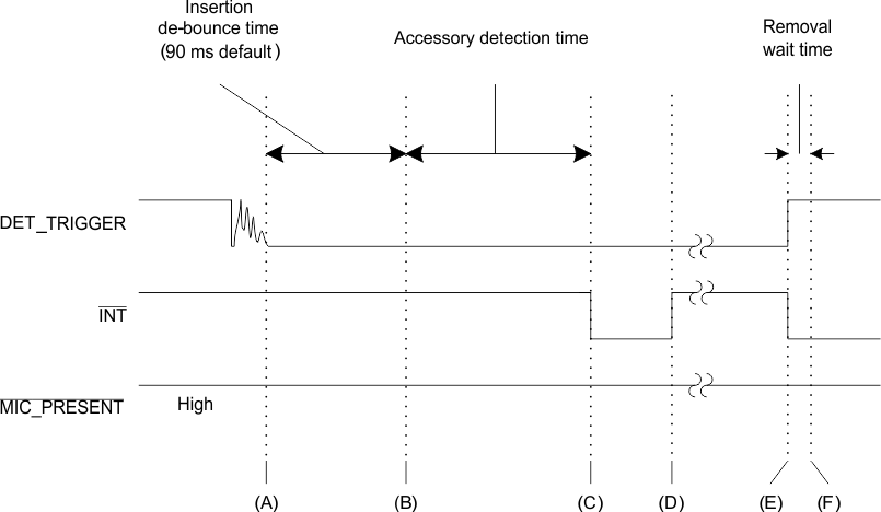
A. (This is the point that DET_TRIGGER has stopped glitching and is fully low. The de-bounce time of 90 ms starts from the point that the pin is constantly below the VIL level. Any time the DET_TRIGGER pin cross the VIH level the de-bounce timer will restart.
B. Point B is the end of the insertion de-bounce time and the beginning of accessory detection.
C. Detection has completed at this point. The switches will be routed before the INT pin is pulled low.
D. INT is cleared after the host reads the interrupt register.
E. The headset is removed here. The switch states will change immediately and INT will be pulled low.
F. After a 50 ms removal de-bounce timer the TS3A227E will go back into sleep mode if manual switch control is not enabled
Figure 1. 3-Pole Accessory
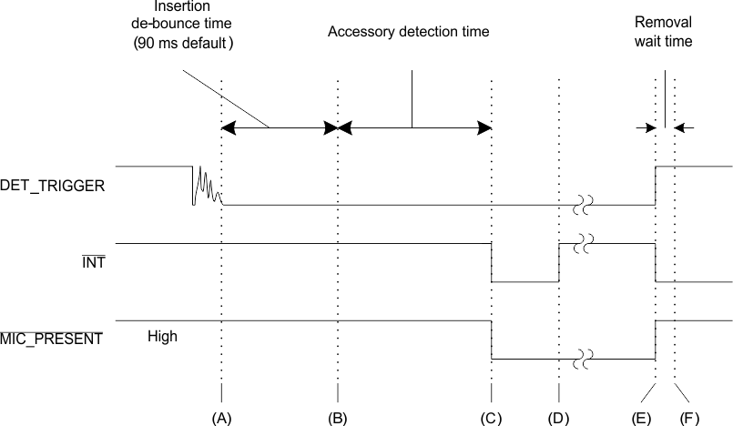
A. This is the point that DET_TRIGGER has stopped glitching and is fully low. The de-bounce time of 90 ms starts from the point that the pin is constantly below the VIL level. Any time the DET_TRIGGER pin cross the VIH level the de-bounce timer will restart.
B. Point B is the end of the insertion de-bounce time and the beginning of accessory detection.
C. Detection has completed at this point. The switches will be routed before the INT and MIC_PRESENT pins are pulled low.
D. INT is cleared after the host reads the interrupt register.
E. The headset is removed here. The switch states will change immediately and INT will be pulled low. The MIC_PRESENT pin will be released.
F. After a 50 ms removal de-bounce timer the TS3A227E will go back into sleep mode if manual switch control is not enabled
Figure 2. 4-Pole Accessory
7.7.1 Removal
A removal event will interrupt any on-going process in the TS3A227E. The following diagram depicts how the device “jumps” during a removal.
If the removal event occurs during the insertion de-bounce period the TS3A227E will jump to the (A) point of the diagram depicted by the green arrow and line.
Any time after point (B) has been reached and the accessory is removed the device jumps to point (E), which includes key press detection. Under Manual Switch Control the switch states will not change.
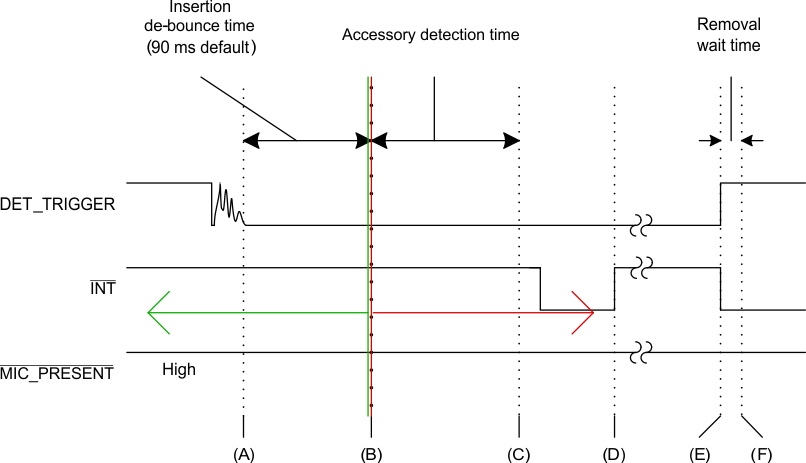 Figure 3. Removal Timing During Insertion
7.8 Typical Characteristics
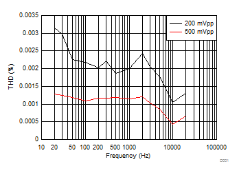 Figure 4. S3PX THD