SBAS484B September   2010  – December 2016 TSC2014

PRODUCTION DATA.  

  1. Features
  2. Applications
  3. Description
  4. Revision History
  5. Pin Configuration and Functions
  6. Electrical Specifications
    1. 6.1  Absolute Maximum Ratings
    2. 6.2  ESD Ratings
    3. 6.3  Thermal Information
    4. 6.4  Recommended Operating Conditions
    5. 6.5  Electrical Characteristics
    6. 6.6  Timing Requirements for : I2C Standard Mode (fSCL = 100 kHz)
    7. 6.7  Timing Requirements for : I2C Fast Mode (fSCL = 400 kHz)
    8. 6.8  Timing Requirements for : I2C High-Speed Mode (fSCL = 1.7 MHz)
    9. 6.9  Timing Requirements for : I2C High-Speed Mode (fSCL = 3.4 MHz)
    10. 6.10 Timing Information
    11. 6.11 Typical Characteristics
  7. Detailed Description
    1. 7.1 Overview
    2. 7.2 Functional Block Diagram
    3. 7.3 Feature Description
      1. 7.3.1 Touch Screen Operation
      2. 7.3.2 4-Wire Touch Screen Coordinate Pair Measurement
      3. 7.3.3 Internal Temperature Sensor
      4. 7.3.4 Analog-to-Digital Converter
        1. 7.3.4.1 Data Format
        2. 7.3.4.2 Reference
        3. 7.3.4.3 Variable Resolution
        4. 7.3.4.4 Conversion Clock and Conversion Time
        5. 7.3.4.5 Touch Detect
        6. 7.3.4.6 Preprocessing
          1. 7.3.4.6.1 Preprocessing—Median Value Filter and Averaging Value Filter
        7. 7.3.4.7 Zone Detection
    4. 7.4 Device Functional Modes
      1. 7.4.1 I2C Interface
        1. 7.4.1.1 I2C Fast or Standard Mode (F/S Mode)
        2. 7.4.1.2 I2C High-Speed Mode (Hs Mode)
      2. 7.4.2 Touch Screen Measurements
        1. 7.4.2.1 Conversion Controlled by TSC2014 Initiated by TSC2014 (TSMode 1)
        2. 7.4.2.2 Conversion Controlled by TSC2014 Initiated by Host (TSMode 2)
        3. 7.4.2.3 Conversion Controlled by Host (TSMode 3)
    5. 7.5 Programming
      1. 7.5.1 Digital Interface
        1. 7.5.1.1 Address Byte
          1. 7.5.1.1.1 Bit D0: R/W
      2. 7.5.2 Start A Write Cycle
      3. 7.5.3 Register Access
      4. 7.5.4 Register Reset
    6. 7.6 Register Maps
      1. 7.6.1 R/W
      2. 7.6.2 Control Byte 0
      3. 7.6.3 Control Byte 1
        1. 7.6.3.1 Touch Screen Scan Function for XYZ or XY
          1. 7.6.3.1.1 C3-C0 = 0000 or 0001
        2. 7.6.3.2 Touch Screen Sensor Connection Tests for X-Axis and Y-Axis
          1. 7.6.3.2.1 C3-C0 = 1001
          2. 7.6.3.2.2 C3-C0 = 1010
        3. 7.6.3.3 Touch Sensor Short-Circuit Test
          1. 7.6.3.3.1 C3-C0 = 1011
          2. 7.6.3.3.2 C3-C0 = 1100
          3. 7.6.3.3.3 RM
          4. 7.6.3.3.4 SWRST
          5. 7.6.3.3.5 STS
      4. 7.6.4 Communication Protocol
        1. 7.6.4.1 Configuration Register 0
          1. 7.6.4.1.1 PSM
          2. 7.6.4.1.2 STS
          3. 7.6.4.1.3 RM
          4. 7.6.4.1.4 CL1, CL0
          5. 7.6.4.1.5 PV2-PV0
          6. 7.6.4.1.6 PR2-PR0
          7. 7.6.4.1.7 SNS2-SNS0
          8. 7.6.4.1.8 DTW
          9. 7.6.4.1.9 LSM
        2. 7.6.4.2 Configuration Register 1
          1. 7.6.4.2.1 TBM3-TBM0
          2. 7.6.4.2.2 BTD2-BTD0
      5. 7.6.5 Configuration Register 2
        1. 7.6.5.1 PINTS1 (default 0)
        2. 7.6.5.2 PINTS0 (default 0)
        3. 7.6.5.3 M1, M0, W1, W0 (default 0000)
        4. 7.6.5.4 TZ1 and TZ0, or AZ1 and AZ0 (default 00)
        5. 7.6.5.5 MAVE (default is 00000)
      6. 7.6.6 Converter Function Select Register
        1. 7.6.6.1 CFN15-CFN13
        2. 7.6.6.2 CFN12-CFN0
        3. 7.6.6.3 DAV Bits
        4. 7.6.6.4 RESET Flag
        5. 7.6.6.5 X CON
        6. 7.6.6.6 Y CON
        7. 7.6.6.7 Y SHR
        8. 7.6.6.8 PDST
        9. 7.6.6.9 ID[1:0]
      7. 7.6.7 Data Registers
        1. 7.6.7.1 X, Y, Z1, Z2, AUX, TEMP1 and TEMP2 Registers
  8. Application and Implementation
    1. 8.1 Application Information
    2. 8.2 Typical Application
      1. 8.2.1 Design Requirements
      2. 8.2.2 Detailed Design Procedure
        1. 8.2.2.1 Auxiliary and Temperature Measurement
      3. 8.2.3 Application Curves
  9. Power Supply Recommendations
    1. 9.1 Power Supply Decoupling Capacitors
  10. 10Layout
    1. 10.1 Layout Guidelines
    2. 10.2 Layout Example
  11. 11Device and Documentation Support
    1. 11.1 Receiving Notification of Documentation Updates
    2. 11.2 Community Resources
    3. 11.3 Trademarks
    4. 11.4 Electrostatic Discharge Caution
    5. 11.5 Glossary
  12. 12Mechanical, Packaging, and Orderable Information

パッケージ・オプション

メカニカル・データ(パッケージ|ピン)
サーマルパッド・メカニカル・データ
発注情報

Pin Configuration and Functions

YZG Package
WCSP-12
(Top View, Solder Bumps on Bottom Side)
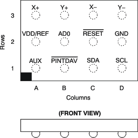
TSC2014 po_wcsp-12_bas484.gif

Pin Assignments

WCSP NAME I/O ANALOG/
DIGITAL
DESCRIPTION
A1 AUX I A Auxiliary channel input
A2 VDD/REF Supply voltage and external reference input
A3 X+ I A X+ channel input
B1 PINTDAV O D Interrupt output. Data available or PENIRQ, depending on setting. Pin polarity is active low.
B2 AD0 I D Address input bit 0
B3 Y+ I A Y+ channel input
C1 SDA I/O D Serial data I/O
C2 RESET I D External hardware-reset input
C3 X– I A X– channel input
D1 SCL I D Serial clock.
D2 GND Ground
D3 Y– I A Y– channel input