JAJSPV3B february 2023 – june 2023 UCC14141-Q1
PRODUCTION DATA
- 1
- 1 特長
- 2 アプリケーション
- 3 概要
- 4 Revision History
- 5 Device Comparison
- 6 Pin Configuration and Functions
- 7 Specifications
- 8 Detailed Description
- 9 Application and Implementation
- 10Device and Documentation Support
- 11Mechanical, Packaging, and Orderable Information
9.2.2.1 Capacitor Selection
The UCC14141-Q1 device creates an isolated output VDD-VEE as its main output. The device also creates a second output COM-VEE, using VDD-VEE as its power source. Because both outputs are isolated from the input, and sharing VEE as the common reference point, the UCC14141-Q1 outputs can be configured as dual-output two-positive, dual-output two-negative, or dual-output one-positive and one-negative. UCC14141-Q1 output can also be used as a single positive output or single negative output.
When the module is configured as dual-output, one-positive output, one-negative output; it is very important to properly select the output capacitor ratios COUT2 and COUT3 to optimize the regulation and avoid causing an over-voltage or under-voltage fault.
| CAPACITOR | VALUE (µF) | NOTES |
|---|---|---|
| CIN | 20 + 0.1 | Place a 20-μF and a 0.1-μF high-frequency decoupling capacitor in parallel close to VIN pins. A capacitance greater than 20 uF can be used to reduce the voltage ripple when the series impedance from the voltage source to the VIN pins is large. |
| COUT1 | 10 + 0.1 | Add a 10-μF and a 0.1-μF capacitor for high-frequency decoupling of (VDD – VEE). Place close to the VDD and VEE pins. A capacitance greater than 10 uF can be used to reduce the output voltage ripple. |
COUT1B | See below | Bulk charge, decoupling output capacitors are required to be located next to the gate driver pins. The COUT2 and COUT3 capacitance ratio is important to optimize the dual output voltage divider accuracy during charge or discharge switching cycles; while the COUT1B capacitor is used to minimize the total capacitance including COUT1B, COUT2, and COUT3 capacitance values. |
| COUT2 | See below | |
| COUT3 | See below |
Output capacitor decoupling is important for optimal gate driver operation. Best high frequency decoupling can be achieved by reducing the parasitic impedance in the charge/discharge path. Using ceramic capacitors with low ESR and low ESL are important, as well as minimizing the trace impedance.
As described in Figure 9-3, a decoupling capacitor COUT1 is required at the VVDD-VEE output pins of the UCC14141-Q1 for high frequency decoupling. COUT2 and COUT3 however, are needed at the gate driver pins for VVDD-COM and VVEE-COM decoupling. The impedance between COUT1 and the COUT2/COUT3 combo prevents the COUT1 from assisting the high frequency decoupling of the gate driver, requiring the COUT2 and COUT3 to take on the full load. The impedance may be contributed from the PCB traces, socket connections, EMI filters, or ferrite beads etc. This causes the COUT2 and in particular the COUT3 to get relatively large achieve a small voltage droop.
 Figure 9-3 Dual Output Schematic with Cout1, Cout2, and Cout3
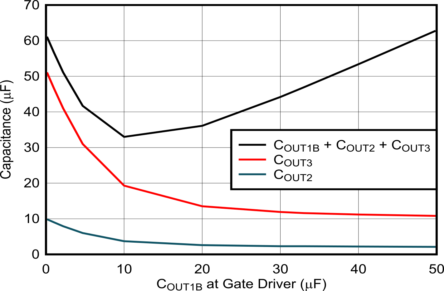
The required COUT2 and COUT3 capacitance can be reduced by introducing a COUT1B capacitor from VVDD-VEE at the gate driver pins next to COUT2 and COUT3 as shown in Figure 9-4. The COUT1B assists with the decoupling total capacitance for both COUT2 and COUT3; thereby reducing the total capacitance (COUT1B + COUT2 +COUT3) needed to achieve the desired voltage droop. Figure 9-5 shows that as COUT1B is increased from “none” to higher COUT1B values, there is a significant reduction in COUT2 and COUT3 and reduction of the total net capacitance, until a point of diminishing returns is reached (a “knee” point) where any additional COUT1B will have a relatively small reduction of COUT2 and COUT3, and starts more significantly increasing the total net capacitance. The optimal COUT1B, COUT2, and COUT3 at the minimum total net capacitance benefit both output capacitor size reduction and BOM cost reduction.
 Figure 9-4 Dual Output Schematic with Cout1, Cout1B, Cout2, and Cout3
 Figure 9-5 Output Capacitance
variation with Cout1B selection
Figure 9-5 Output Capacitance
variation with Cout1B selectionTo calculate COUT1B, COUT2, and COUT3, we calculate the equivalent (VDD-COM) capacitance, which is equal to the series capacitance of COUT1B and COUT3 in parallel with COUT2. This equivalent (VDD-VEE) capacitance will be sized to limit the predetermined (VDD-COM) discharge voltage drop when the power switch (SiC or IGBT) gate charge is turned-on.
The COUT2 over COUT3 ratio is defined as a coefficient of K23,which is the multiplication of a voltage divider ratio along with a ratio of differential current. The voltage divider ratio is from the series configuration of the two capacitors. The current divider ratio is calculated based on the charge current through the two capacitors. IMAX_POWER is the maximum instantaneous current from the power module during the burst on-time, which can be obtained from dividing the maximum power on the datasheet SOA curve at TA of 25°C by VVDD-VEE. IVDD-COM is the total quiescent current between VDD and COM. For gate driver as example, IVDD-VEE is the current consumption without switching. ICOM-VEE is the total quiescent current between COM and VEE. Based on KCL, the differential current charging up COUT2 during the burst on-time is (IMAX_POWER - IVDD-COM), and the one charging up COUT3 is (IMAX_POWER - ICOM-VEE).
where
Next, plugging the above COUT3 expression into the Equation 1 we get
The total decoupling capacitance close to the point of load (COUT_Total) is the summation of COUT1B, COUT2 and COUT3. The goal is to find a smallest COUT1B to reduce COUT_Total to the minimum for BOM cost and footprint saving, while retaining the desired load transient performance. The optimal COUT1B can be calculated by solving the partial derivative of COUT_Total equal to 0.
After that, solving Equation 5 including Equation 7, COUT2 can be solved as