JAJSE88F November 2017 – February 2024 UCC21220 , UCC21220A
PRODUCTION DATA
- 1
- 1 特長
- 2 アプリケーション
- 3 概要
- 4 Device Comparison Table
- 5 Pin Configuration and Functions
-
6 Specifications
- 6.1 Absolute Maximum Ratings
- 6.2 ESD Ratings
- 6.3 Recommended Operating Conditions
- 6.4 Thermal Information
- 6.5 Power Ratings
- 6.6 Insulation Specifications
- 6.7 Safety-Related Certifications
- 6.8 Safety-Limiting Values
- 6.9 Electrical Characteristics
- 6.10 Switching Characteristics
- 6.11 Thermal Derating Curves
- 6.12 Typical Characteristics
- 7 Parameter Measurement Information
- 8 Detailed Description
-
9 Application and Implementation
- 9.1 Application Information
- 9.2
Typical Application
- 9.2.1 Design Requirements
- 9.2.2
Detailed Design Procedure
- 9.2.2.1 Designing INA/INB Input Filter
- 9.2.2.2 Select External Bootstrap Diode and its Series Resistor
- 9.2.2.3 Gate Driver Output Resistor
- 9.2.2.4 Estimating Gate Driver Power Loss
- 9.2.2.5 Estimating Junction Temperature
- 9.2.2.6 Selecting VCCI, VDDA/B Capacitor
- 9.2.2.7 Application Circuits with Output Stage Negative Bias
- 9.2.3 Application Curves
- 10Power Supply Recommendations
- 11Layout
- 12Device and Documentation Support
- 13Revision History
- 14Mechanical, Packaging, and Orderable Information
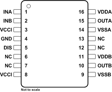
5 Pin Configuration and Functions
 Figure 5-1 D
Package16-Pin SOICTop View
Figure 5-1 D
Package16-Pin SOICTop ViewTable 5-1 Pin Functions
| PIN | NO. | TYPE(1) | DESCRIPTION |
|---|---|---|---|
| DIS | 5 | I | Disables both driver outputs if asserted high, enables if set low or left open. This pin is pulled low internally if left open. It is recommended to tie this pin to ground if not used to achieve better noise immunity. Bypass using a ≈ 1-nF low ESR/ESL capacitor close to DIS pin when connecting to a µC with distance. |
| GND | 4 | P | Primary-side ground reference. All signals in the primary side are referenced to this ground. |
| INA | 1 | I | Input signal for A channel. INA input has a TTL/CMOS compatible input threshold. This pin is pulled low internally if left open. It is recommended to tie this pin to ground if not used to achieve better noise immunity. |
| INB | 2 | I | Input signal for B channel. INB input has a TTL/CMOS compatible input threshold. This pin is pulled low internally if left open. It is recommended to tie this pin to ground if not used to achieve better noise immunity. |
| NC | 6 | No internal connection | |
| 7 | |||
| 12 | |||
| 13 | |||
| OUTA | 15 | O | Output of driver A. Connect to the gate of the A channel FET or IGBT. |
| OUTB | 10 | O | Output of driver B. Connect to the gate of the B channel FET or IGBT. |
| VCCI | 3 | P | Primary-side supply voltage. Locally decoupled to GND using a low ESR/ESL capacitor located as close to the device as possible. |
| VCCI | 8 | P | This pin is internally shorted to pin 3. |
| VDDA | 16 | P | Secondary-side power for driver A. Locally decoupled to VSSA using a low ESR/ESL capacitor located as close to the device as possible. |
| VDDB | 11 | P | Secondary-side power for driver B. Locally decoupled to VSSB using a low ESR/ESL capacitor located as close to the device as possible. |
| VSSA | 14 | P | Ground for secondary-side driver A. Ground reference for secondary side A channel. |
| VSSB | 9 | P | Ground for secondary-side driver B. Ground reference for secondary side B channel. |
(1) P = power, G = ground, I = input, O = output