JAJSE88G November 2017 – November 2024 UCC21220 , UCC21220A
PRODUCTION DATA
- 1
- 1 特長
- 2 アプリケーション
- 3 概要
- 4 Device Comparison Table
- 5 Pin Configuration and Functions
- 6 Specifications
- 7 Parameter Measurement Information
- 8 Detailed Description
-
9 Application and Implementation
- 9.1 Application Information
- 9.2
Typical Application
- 9.2.1 Design Requirements
- 9.2.2
Detailed Design Procedure
- 9.2.2.1 Designing INA/INB Input Filter
- 9.2.2.2 Select External Bootstrap Diode and its Series Resistor
- 9.2.2.3 Gate Driver Output Resistor
- 9.2.2.4 Estimating Gate Driver Power Loss
- 9.2.2.5 Estimating Junction Temperature
- 9.2.2.6 Selecting VCCI, VDDA/B Capacitor
- 9.2.2.7 Application Circuits with Output Stage Negative Bias
- 9.2.3 Application Curves
- 10Power Supply Recommendations
- 11Layout
- 12Device and Documentation Support
- 13Revision History
- 14Mechanical, Packaging, and Orderable Information
パッケージ・オプション
デバイスごとのパッケージ図は、PDF版データシートをご参照ください。
メカニカル・データ(パッケージ|ピン)
- D|16
サーマルパッド・メカニカル・データ
発注情報
9.2.2.3 Gate Driver Output Resistor
The external gate driver resistors, RON/ROFF, are used to:
- Limit ringing caused by parasitic inductances/capacitances.
- Limit ringing caused by high voltage/current switching dv/dt, di/dt, and body-diode reverse recovery.
- Fine-tune gate drive strength, i.e. peak sink and source current to optimize the switching loss.
- Reduce electromagnetic interference (EMI).
As mentioned in Section 8.3.4, the UCC21220 and UCC21220A have a pull-up structure with a P-channel MOSFET and an additional pull-up N-channel MOSFET in parallel. The combined peak source current is 4 A. Therefore, the peak source current can be predicted with Equation 2 and Equation 3:


where
- RON: External turn-on resistance.
- RGFET_INT: Power transistor internal gate resistance, found in the power transistor datasheet.
- IO+ = Peak source current – The minimum value between 4 A, the gate driver peak source current, and the calculated value based on the gate drive loop resistance.
In this example:


Therefore, the high-side and low-side peak source current is 2.3 A and 2.5 A respectively. Similarly, the peak sink current can be calculated with Equation 6 and Equation 7:


where
- ROFF: External turn-off resistance, ROFF=0 in this example;
- VGDF: The anti-parallel diode forward voltage drop which is in series with ROFF. The diode in this example is an MSS1P4.
- IO-: Peak sink current – the minimum value between 6 A, the gate driver peak sink current, and the calculated value based on the gate drive loop resistance.
In this example,
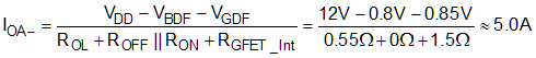

Therefore, the high-side and low-side peak sink current is 5.0 A and 5.4A respectively.
Importantly, the estimated peak current is also influenced by PCB layout and load capacitance. Parasitic inductance in the gate driver loop can slow down the peak gate drive current and introduce overshoot and undershoot. Therefore, it is strongly recommended that the gate driver loop should be minimized. On the other hand, the peak source/sink current is dominated by loop parasitics when the load capacitance (CISS) of the power transistor is very small (typically less than 1 nF), because the rising and falling time is too small and close to the parasitic ringing period.