JAJSFJ9B December 2017 – October 2019 UCC28064A
PRODUCTION DATA.
- 1 特長
- 2 アプリケーション
- 3 概要
- 4 改訂履歴
- 5 概要(続き)
- 6 Pin Configuration and Functions
- 7 Specifications
-
8 Detailed Description
- 8.1 Overview
- 8.2 Functional Block Diagram
- 8.3
Feature Description
- 8.3.1 Principles of Operation
- 8.3.2 Natural Interleaving
- 8.3.3 On-Time Control, Maximum Frequency Limiting, Restart Timer and Input Voltage Feed-Forward compensation
- 8.3.4 Distortion Reduction
- 8.3.5 Zero-Current Detection and Valley Switching
- 8.3.6 Phase Management and Light-Load Operation
- 8.3.7 Burst Mode Operation
- 8.3.8 External Disable
- 8.3.9 Improved Error Amplifier
- 8.3.10 Soft Start
- 8.3.11 Brownout Protection
- 8.3.12 Line Dropout Detection
- 8.3.13 VREF
- 8.3.14 VCC
- 8.3.15
System Level Protections
- 8.3.15.1 Failsafe OVP - Output Over-voltage Protection
- 8.3.15.2 Overcurrent Protection
- 8.3.15.3 Open-Loop Protection
- 8.3.15.4 VCC Undervoltage Lock-Out (UVLO) Protection
- 8.3.15.5 Phase-Fail Protection
- 8.3.15.6 CS - Open, TSET - Open and Short Protection
- 8.3.15.7 Thermal Shutdown Protection
- 8.3.15.8 Fault Logic Diagram
- 8.4 Device Functional Modes
-
9 Application and Implementation
- 9.1 Application Information
- 9.2
Typical Application
- 9.2.1 Design Requirements
- 9.2.2
Detailed Design Procedure
- 9.2.2.1 Custom Design With WEBENCH® Tools
- 9.2.2.2 Inductor Selection
- 9.2.2.3 ZCD Resistor Selection RZA, RZB
- 9.2.2.4 HVSEN
- 9.2.2.5 Output Capacitor Selection
- 9.2.2.6 Selecting RS For Peak Current Limiting
- 9.2.2.7 Power Semiconductor Selection (Q1, Q2, D1, D2)
- 9.2.2.8 Brownout Protection
- 9.2.2.9 Converter Timing
- 9.2.2.10 Programming VOUT
- 9.2.2.11 Voltage Loop Compensation
- 9.2.3 Application Curves
- 10Power Supply Recommendations
- 11Layout
- 12Package Option Addendum
- 13デバイスおよびドキュメントのサポート
- 14メカニカル、パッケージ、および注文情報
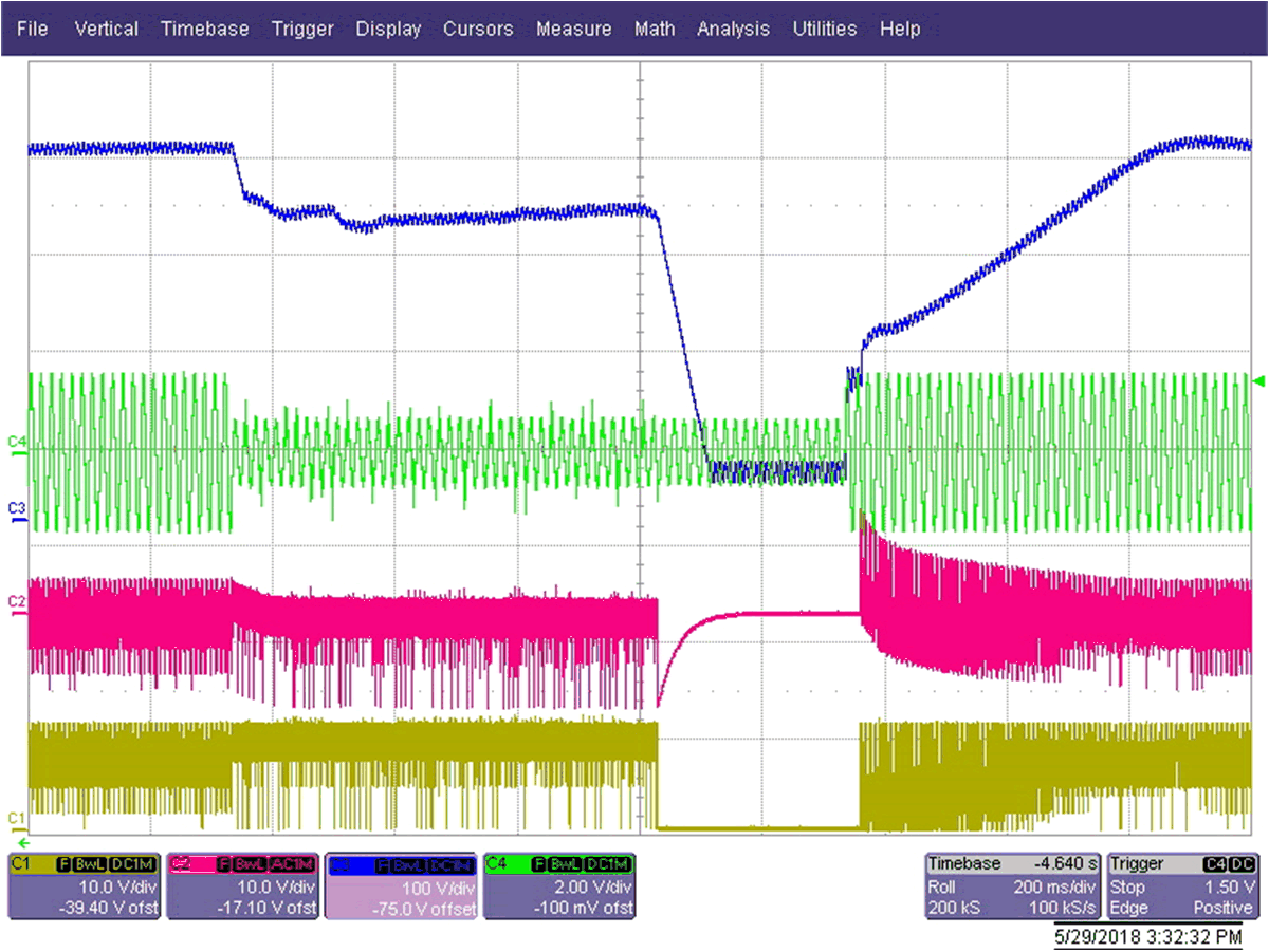
9.2.3.2 Brownout Protection
The UCC28064A has a brownout protection that shuts down both gate drives (GDA and GDB) when the VINAC pin detects that the RMS input voltage is too low. Figure 35.

| CH1 = VGDA | CH2 = VGDB |
| CH3 = VOUT | CH3 = VIN |