JAJS381E September 2009 – September 2018 TPS54218
PRODUCTION DATA.
- 1 特長
- 2 アプリケーション
- 3 概要
- 4 改訂履歴
- 5 概要(続き)
- 6 Pin Configuration and Functions
- 7 Specifications
-
8 Detailed Description
- 8.1 Overview
- 8.2 Functional Block Diagram
- 8.3
Feature Description
- 8.3.1 Fixed Frequency PWM Control
- 8.3.2 Slope Compensation and Output Current
- 8.3.3 Bootstrap Voltage (Boot) and Low Dropout Operation
- 8.3.4 Error Amplifier
- 8.3.5 Voltage Reference
- 8.3.6 Adjusting the Output Voltage
- 8.3.7 Enable and Adjusting Undervoltage Lockout
- 8.3.8 Soft-Start Pin
- 8.3.9 Sequencing
- 8.3.10 Constant Switching Frequency and Timing Resistor (RT/CLK Pin)
- 8.3.11 Overcurrent Protection
- 8.3.12 Frequency Shift
- 8.3.13 Reverse Overcurrent Protection
- 8.3.14 Synchronize Using the RT/CLK Pin
- 8.3.15 Power Good (PWRGD Pin)
- 8.3.16 Overvoltage Transient Protection
- 8.3.17 Thermal Shutdown
- 8.4 Device Functional Modes
-
9 Application and Implementation
- 9.1 Application Information
- 9.2
Typical Application
- 9.2.1 Design Requirements
- 9.2.2
Detailed Design Procedure
- 9.2.2.1 Step One: Select the Switching Frequency
- 9.2.2.2 Step Two: Select the Output Inductor
- 9.2.2.3 Step Three: Choose the Output Capacitor
- 9.2.2.4 Step Four: Select the Input Capacitor
- 9.2.2.5 Step Five: Minimum Load DC COMP Voltage
- 9.2.2.6 Step Six: Choose the Soft-Start Capacitor
- 9.2.2.7 Step Seven: Select the Bootstrap Capacitor
- 9.2.2.8 Step Eight: Undervoltage Lockout Threshold
- 9.2.2.9 Step Nine: Select Output Voltage and Feedback Resistors
- 9.2.2.10 Step 10: Select Loop Compensation Components
- 9.2.2.11 Power Dissipation Estimate
- 9.2.3 Application Curves
- 10Power Supply Recommendations
- 11Layout
- 12デバイスおよびドキュメントのサポート
- 13メカニカル、パッケージ、および注文情報
7.6 Typical Characteristics
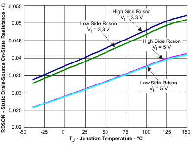 Figure 1. High-Side and Low-Side On-Resistance vs Junction Temperature
 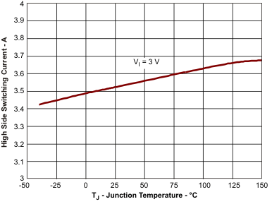 Figure 3. High-Side Current Limit vs Junction Temperature
 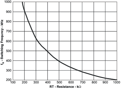 Figure 5. Switching Frequency vs RT Resistance Low Frequency Range
 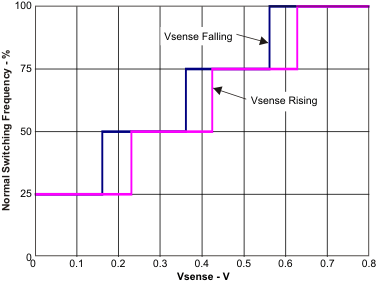 Figure 7. Switching Frequency vs Vsense
 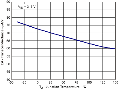 Figure 9. Transconductance (Soft-Start) vs Junction Temperature
 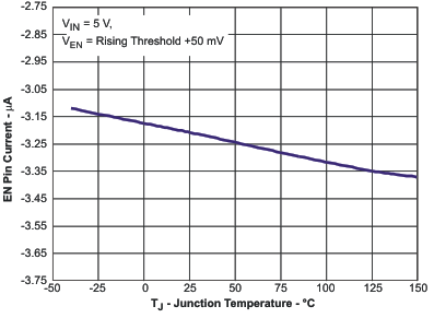 Figure 11. Pin Current vs Junction Temperature
 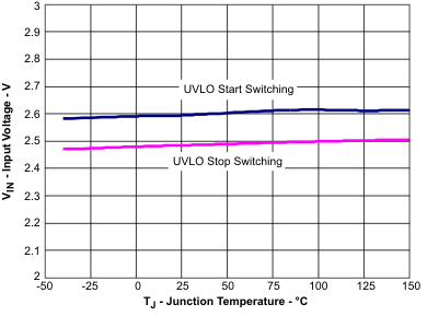 Figure 15. Input Voltage vs Junction Temperature
 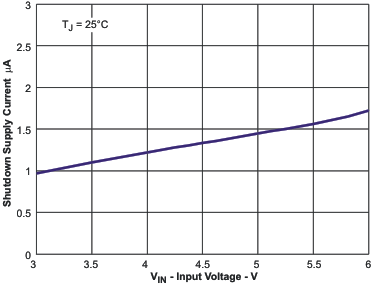 Figure 17. Shutdown Supply Current vs Input Voltage
 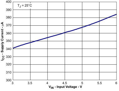 Figure 19. Supply Current vs Input Voltage
 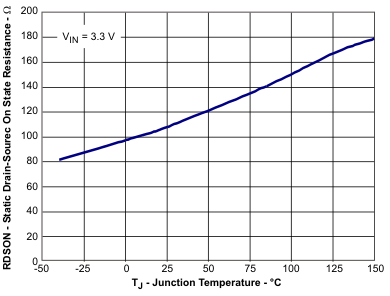 Figure 21. PWRGD On Resistance vs Junction Temperature
 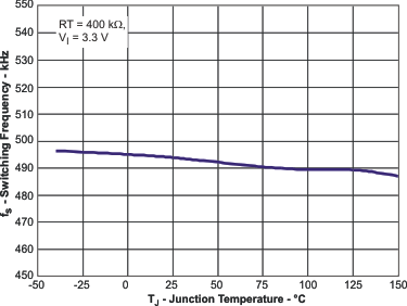 Figure 2. Switching Frequency vs Junction Temperature
 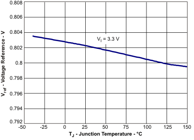 Figure 4. Voltage Reference vs Junction Temperature
 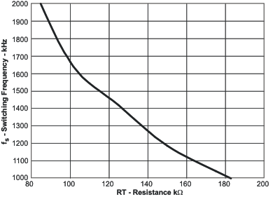 Figure 6. Switching Frequency vs RT Resistance High Frequency Range
 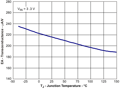 Figure 8. Transconductance vs Junction Temperature
 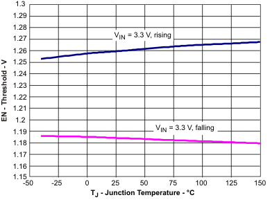 Figure 10. Enable Pin Voltage vs Junction Temperature
 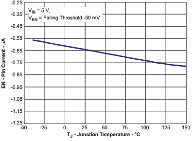 Figure 12. Pin Current vs Junction Temperature
 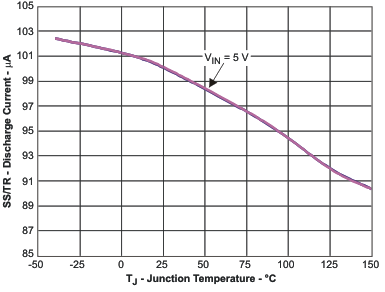 Figure 14. Discharge Current vs Junction Temperature
 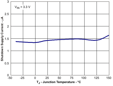 Figure 16. Shutdown Supply Current vs Junction Temperature
 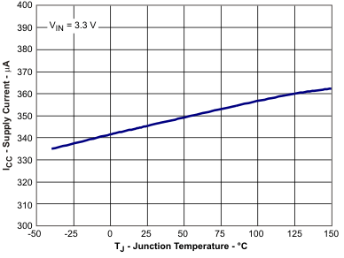 Figure 18. Supply Current vs Junction Temperature
 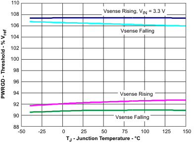 Figure 20. PWRGD Threshold vs Junction Temperature