JAJSDR4C August   2017  – May 2019 INA1650-Q1 , INA1651-Q1

PRODUCTION DATA.  

  1. 特長
  2. アプリケーション
    1.     簡略化された内部回路図
  3. 概要
    1.     CMRRヒストグラム(5746チャネル)
  4. 改訂履歴
  5. Pin Configuration and Functions
    1.     Pin Functions: INA1650-Q1
    2.     Pin Functions: INA1651-Q1
  6. Specifications
    1. 6.1 Absolute Maximum Ratings
    2. 6.2 ESD Ratings
    3. 6.3 Recommended Operating Conditions
    4. 6.4 Thermal Information
    5. 6.5 Electrical Characteristics:
    6. 6.6 Typical Characteristics
  7. Detailed Description
    1. 7.1 Overview
    2. 7.2 Functional Block Diagram
    3. 7.3 Feature Description
      1. 7.3.1 Audio Signal Path
      2. 7.3.2 Supply Divider
      3. 7.3.3 EMI Rejection
      4. 7.3.4 Electrical Overstress
      5. 7.3.5 Thermal Shutdown
    4. 7.4 Device Functional Modes
      1. 7.4.1 Single-Supply Operation
  8. Application and Implementation
    1. 8.1 Application Information
      1. 8.1.1 Input Common-Mode Range
      2. 8.1.2 Common-Mode Input Impedance
      3. 8.1.3 Start-Up Time in Single-Supply Applications
      4. 8.1.4 Input AC Coupling
      5. 8.1.5 Supply Divider Capacitive Loading
    2. 8.2 Typical Applications
      1. 8.2.1 Line Receiver for Differential Audio Signals in a Split-Supply System
        1. 8.2.1.1 Design Requirements
        2. 8.2.1.2 Detailed Design Procedure
        3. 8.2.1.3 Application Curves
      2. 8.2.2 Two-Channel Microphone Input for Automotive Infotainment Systems
      3. 8.2.3 TRS Audio Interface in Single-Supply Applications
  9. Power Supply Recommendations
  10. 10Layout
    1. 10.1 Layout Guidelines
    2. 10.2 Layout Example
  11. 11デバイスおよびドキュメントのサポート
    1. 11.1 デバイス・サポート
      1. 11.1.1 開発サポート
        1. 11.1.1.1 TINA-TI(無料のダウンロード・ソフトウェア)
        2. 11.1.1.2 TI Precision Designs
    2. 11.2 ドキュメントのサポート
      1. 11.2.1 関連資料
    3. 11.3 ドキュメントの更新通知を受け取る方法
    4. 11.4 コミュニティ・リソース
    5. 11.5 商標
    6. 11.6 静電気放電に関する注意事項
    7. 11.7 Glossary
  12. 12メカニカル、パッケージ、および注文情報

Audio Signal Path

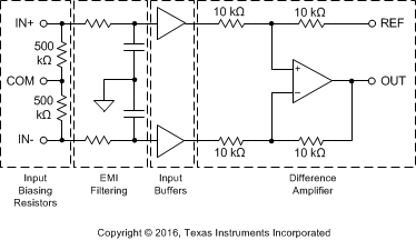
Figure 39 highlights the basic elements present in the audio signal pathway of the INA165x-Q1 line receivers. The primary elements are input biasing resistors, electromagnetic interference (EMI) filtering, input buffers, and a difference amplifier. The primary role of an audio line receiver is to convert a differential input signal into a single-ended output signal while rejecting noise that is common to both inputs (common-mode noise). The difference amplifier (which consists of an op amp and four matched 10-kΩ resistors) accomplishes this task. The basic transfer function of the circuit is shown in Equation 1:

Equation 1. INA1650-Q1 INA1651-Q1 FBD_eq_001.gif
INA1650-Q1 INA1651-Q1 FD_D001.gifFigure 39. INA165x-Q1 Audio Signal Path (Single Channel Shown)

The input buffers prevent external resistances (such as those from the PCB, connectors, or cables) from ruining the precise matching of the internal 10-kΩ resistors that degrade the high common-mode rejection of the difference amplifier. As is typical of many amplifiers, a small bias current flows into or out of the buffer amplifier inputs. This current must flow to a common potential for the buffer to function properly. The input biasing resistors provide an internal pathway for this current to the COM pin. The COM pin connects to ground in a dual-supply system, or to the output of the internal supply divider, VMID(OUT), in single-supply applications. Finally, EMI filtering is added to the input buffers to prevent high-frequency interference signals from propagating through the audio signal pathway.