JAJSEE2C January   2018  – December 2019 MSP430FR2512 , MSP430FR2522

PRODUCTION DATA.  

  1. 1デバイスの概要
    1. 1.1 特長
    2. 1.2 アプリケーション
    3. 1.3 概要
    4. 1.4 機能ブロック図
  2. 2改訂履歴
  3. 3Device Comparison
    1. 3.1 Related Products
  4. 4Terminal Configuration and Functions
    1. 4.1 Pin Diagrams
    2. 4.2 Pin Attributes
    3. 4.3 Signal Descriptions
    4. 4.4 Pin Multiplexing
    5. 4.5 Buffer Types
    6. 4.6 Connection of Unused Pins
  5. 5Specifications
    1. 5.1       Absolute Maximum Ratings
    2. 5.2       ESD Ratings
    3. 5.3       Recommended Operating Conditions
    4. 5.4       Active Mode Supply Current Into VCC Excluding External Current
    5. 5.5       Active Mode Supply Current Per MHz
    6. 5.6       Low-Power Mode (LPM0) Supply Currents Into VCC Excluding External Current
    7. 5.7       Low-Power Mode (LPM3, LPM4) Supply Currents (Into VCC) Excluding External Current
    8. 5.8       Low-Power Mode (LPMx.5) Supply Currents (Into VCC) Excluding External Current
    9. 5.9       Typical Characteristics - Low-Power Mode Supply Currents
    10. Table 5-1 Typical Characteristics – Current Consumption Per Module
    11. 5.10      Thermal Resistance Characteristics
    12. 5.11      Timing and Switching Characteristics
      1. 5.11.1  Power Supply Sequencing
        1. Table 5-2 PMM, SVS and BOR
      2. 5.11.2  Reset Timing
        1. Table 5-3 Wake-up Times From Low-Power Modes and Reset
      3. 5.11.3  Clock Specifications
        1. Table 5-4 XT1 Crystal Oscillator (Low Frequency)
        2. Table 5-5 DCO FLL, Frequency
        3. Table 5-6 DCO Frequency
        4. Table 5-7 REFO
        5. Table 5-8 Internal Very-Low-Power Low-Frequency Oscillator (VLO)
        6. Table 5-9 Module Oscillator (MODOSC)
      4. 5.11.4  Digital I/Os
        1. Table 5-10 Digital Inputs
        2. Table 5-11 Digital Outputs
        3. 5.11.4.1   Typical Characteristics – Outputs at 3 V and 2 V
      5. 5.11.5  VREF+ Built-in Reference
        1. Table 5-12 VREF+
      6. 5.11.6  Timer_A
        1. Table 5-13 Timer_A
      7. 5.11.7  eUSCI
        1. Table 5-14 eUSCI (UART Mode) Clock Frequency
        2. Table 5-15 eUSCI (UART Mode)
        3. Table 5-16 eUSCI (SPI Master Mode) Clock Frequency
        4. Table 5-17 eUSCI (SPI Master Mode)
        5. Table 5-18 eUSCI (SPI Slave Mode)
        6. Table 5-19 eUSCI (I2C Mode)
      8. 5.11.8  ADC
        1. Table 5-20 ADC, Power Supply and Input Range Conditions
        2. Table 5-21 ADC, 10-Bit Timing Parameters
        3. Table 5-22 ADC, 10-Bit Linearity Parameters
      9. 5.11.9  CapTIvate
        1. Table 5-23 CapTIvate Electrical Characteristics
        2. Table 5-24 CapTIvate Signal-to-Noise Ratio Characteristics
      10. 5.11.10 FRAM
        1. Table 5-25 FRAM
      11. 5.11.11 Debug and Emulation
        1. Table 5-26 JTAG, Spy-Bi-Wire Interface
        2. Table 5-27 JTAG, 4-Wire Interface
  6. 6Detailed Description
    1. 6.1  Overview
    2. 6.2  CPU
    3. 6.3  Operating Modes
    4. 6.4  Interrupt Vector Addresses
    5. 6.5  Bootloader (BSL)
    6. 6.6  JTAG Standard Interface
    7. 6.7  Spy-Bi-Wire Interface (SBW)
    8. 6.8  FRAM
    9. 6.9  Memory Protection
    10. 6.10 Peripherals
      1. 6.10.1  Power-Management Module (PMM)
      2. 6.10.2  Clock System (CS) and Clock Distribution
      3. 6.10.3  General-Purpose Input/Output Port (I/O)
      4. 6.10.4  Watchdog Timer (WDT)
      5. 6.10.5  System (SYS) Module
      6. 6.10.6  Cyclic Redundancy Check (CRC)
      7. 6.10.7  Enhanced Universal Serial Communication Interface (eUSCI_A0, eUSCI_B0)
      8. 6.10.8  Timers (Timer0_A3, Timer1_A3)
      9. 6.10.9  Hardware Multiplier (MPY)
      10. 6.10.10 Backup Memory (BAKMEM)
      11. 6.10.11 Real-Time Clock (RTC)
      12. 6.10.12 10-Bit Analog-to-Digital Converter (ADC)
      13. 6.10.13 CapTIvate Technology
      14. 6.10.14 Embedded Emulation Module (EEM)
    11. 6.11 Input/Output Diagrams
      1. 6.11.1 Port P1 (P1.0 to P1.7) Input/Output With Schmitt Trigger
      2. 6.11.2 Port P2 (P2.0 to P2.6) Input/Output With Schmitt Trigger
    12. 6.12 Device Descriptors
    13. 6.13 Memory
      1. 6.13.1 Memory Organization
      2. 6.13.2 Peripheral File Map
    14. 6.14 Identification
      1. 6.14.1 Revision Identification
      2. 6.14.2 Device Identification
      3. 6.14.3 JTAG Identification
  7. 7Applications, Implementation, and Layout
    1. 7.1 Device Connection and Layout Fundamentals
      1. 7.1.1 Power Supply Decoupling and Bulk Capacitors
      2. 7.1.2 External Oscillator
      3. 7.1.3 JTAG
      4. 7.1.4 Reset
      5. 7.1.5 Unused Pins
      6. 7.1.6 General Layout Recommendations
      7. 7.1.7 Do's and Don'ts
    2. 7.2 Peripheral- and Interface-Specific Design Information
      1. 7.2.1 ADC Peripheral
        1. 7.2.1.1 Partial Schematic
        2. 7.2.1.2 Design Requirements
        3. 7.2.1.3 Layout Guidelines
      2. 7.2.2 CapTIvate Peripheral
        1. 7.2.2.1 Device Connection and Layout Fundamentals
        2. 7.2.2.2 Measurements
          1. 7.2.2.2.1 SNR
          2. 7.2.2.2.2 Sensitivity
          3. 7.2.2.2.3 Power
    3. 7.3 CapTIvate Technology Evaluation
  8. 8デバイスおよびドキュメントのサポート
    1. 8.1  使い始めと次の手順
    2. 8.2  デバイスの項目表記
    3. 8.3  ツールとソフトウェア
    4. 8.4  ドキュメントのサポート
    5. 8.5  関連リンク
    6. 8.6  Community Resources
    7. 8.7  商標
    8. 8.8  静電気放電に関する注意事項
    9. 8.9  Export Control Notice
    10. 8.10 Glossary
  9. 9メカニカル、パッケージ、および注文情報

Timers (Timer0_A3, Timer1_A3)

The Timer0_A3 and Timer1_A3 modules are 16-bit timers and counters with three capture/compare registers each. Each timer supports multiple captures or compares, PWM outputs, and interval timing (see Figure 6-2). Each timer has extensive interrupt capabilities. Interrupts may be generated from the counter on overflow conditions and from each of the capture/compare registers. The CCR0 registers on both Timer0_A3 and Timer1_A3 are not externally connected and can only be used for hardware period timing and interrupt generation. In Up mode, they can be used to set the overflow value of the counter.
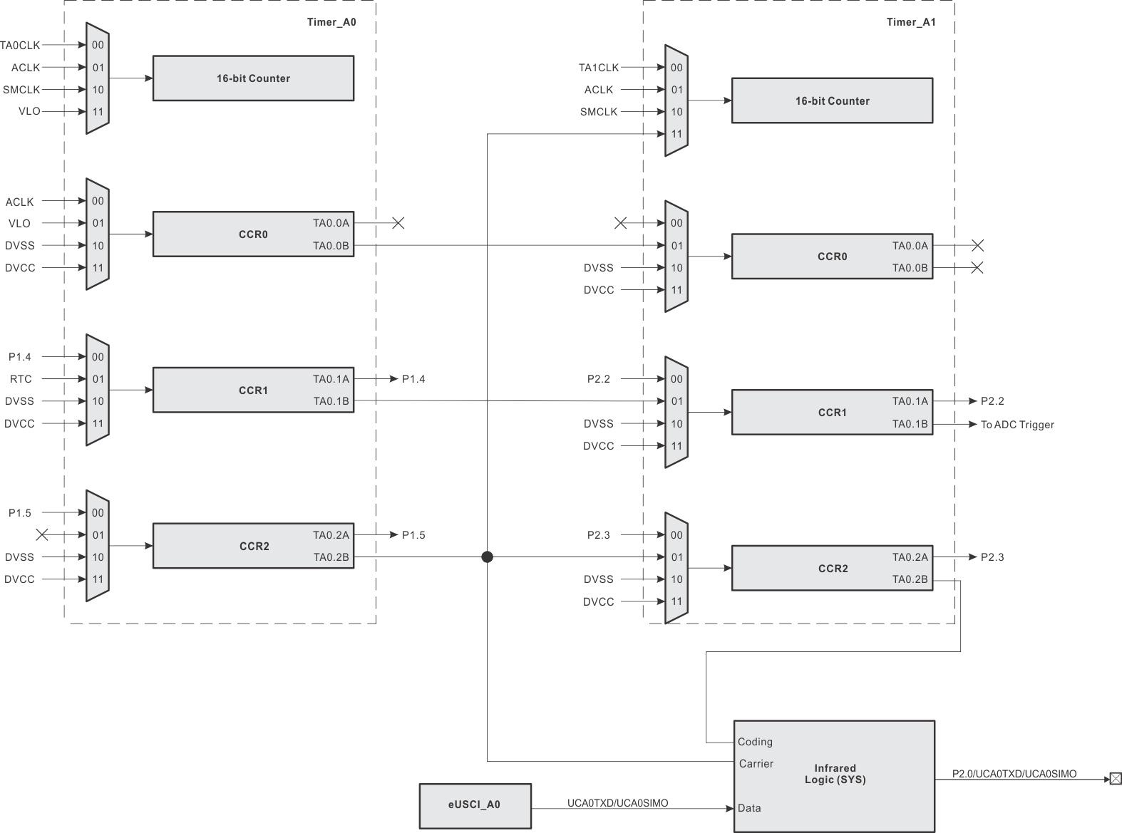
MSP430FR2522 MSP430FR2512 SLASEE4_TA_Connections.gifFigure 6-2 Timer0_A3 and Timer1_A3 Signal Connections

The interconnection of Timer0_A3 and Timer1_A3 can be used to modulate the eUSCI_A pin of UCA0TXD/UCA0SIMO in either ASK or FSK mode, with which a user can easily acquire a modulated infrared command for directly driving an external IR diode. The IR functions are fully controlled by SYS configuration registers 1 including IREN (enable), IRPSEL (polarity select), IRMSEL (mode select), IRDSSEL (data select), and IRDATA (data) bits. For more information, see the SYS chapter in the MP430FR4xx and MP430FR2xx Family User's Guide.