JAJU857 December 2022
- 概要
- リソース
- 特長
- アプリケーション
- 5
- 1System Description
- 2System Overview
-
3Hardware, Software, Testing Requirements, and Test Results
- 3.1
Hardware
- 3.1.1 Board Overview
- 3.1.2 Filter Stage
- 3.1.3 Differential to Single-Ended Converter
- 3.1.4 Low-Pass Filter
- 3.1.5 Full-Wave Rectifier
- 3.1.6 DC Offset Circuit
- 3.1.7 Auto-Oscillation Circuit
- 3.1.8 DRV8220 H-Bridge
- 3.1.9 Saturation Detection Circuit
- 3.1.10 H-Bridge Controlled by DFF
- 3.1.11 MCU Selection
- 3.1.12 Move Away From Timer Capture
- 3.1.13 Differentiating DC and AC From the Same Signal
- 3.1.14 Fluxgate Sensor
- 3.2 Software Requirements
- 3.3 Test Setup
- 3.4 Test Results
- 3.5 Fault Response Results
- 3.1
Hardware
- 4Design and Documentation Support
- 5About the Author
3.1.3 Differential to Single-Ended Converter
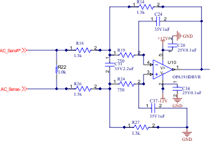
The differential to single-end conversion is performed by the first part of the signal chain. The first op amp converts the differential signal across the fluxgate burden resistor to a single-ended signal. This simplifies later signal conditioning and allows the ADC to read a ground referenced signal. R22 is the burden resistor across the coils of the fluxgate sensor.
Impedance matching to op amp inputs is important to minimize error. Mismatched impedance adds error to the fault detection signal. Trace from R22 to U10 can be similar to reduce error. To increase the ground fault signal, replace R18 and R26 with buffer op amps or resistors an order of magnitude larger.
A higher impedance relative to the burden resistor (R22) gives a higher ground fault signal due to the resistor divider effect.
The first filter stage in Figure 3-4 is used to convert the differential signal across the burden resistor to a single-ended signal. These interface between the burden resistor (R22) of the fluxgate sensor and the TIDA-010237.
 Figure 3-4 Differential to Single-Ended Schematic