JAJU880 December 2022
3.3.4 Protection
The design integrates a full set of battery cell protections, including: cell overvoltage, cell undervoltage, two levels of overcurrent discharge, overcurrent charge, discharge short circuit, and overtemperature and undertemperature protections. Furthermore, this design also monitors lots of system-level faults, including: cell open wire, host watch dog, charge and discharge MOSFETs faults, MOSFETs overtemperature, and so on. Some of the protections were tested in a TI lab.
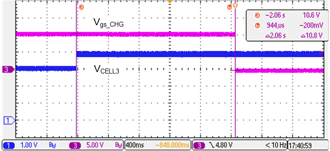 Figure 3-7 Cell Overvoltage Protection
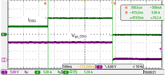 Figure 3-9 Overcurrent Discharge Protection
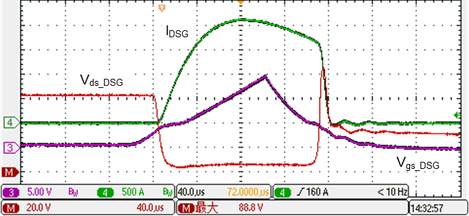 Figure 3-11 Short-Circuit Discharge Protection
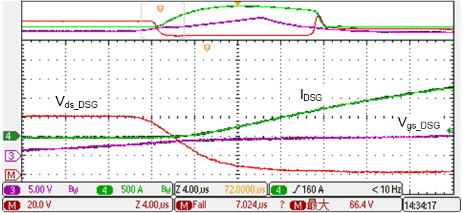 Figure 3-13 Short-Circuit Discharge Protection - MOSFET On
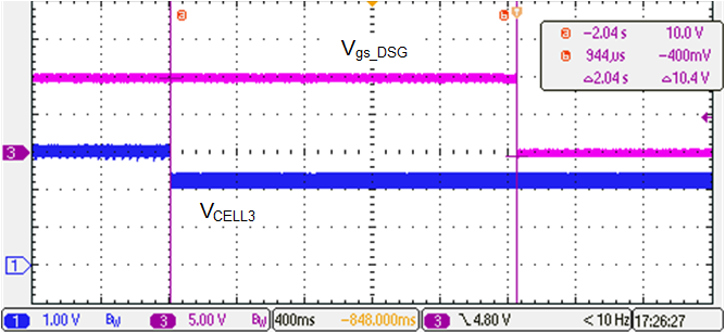 Figure 3-8 Cell Undervoltage Protection
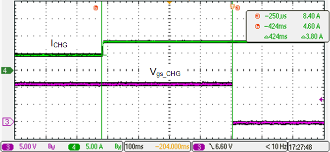 Figure 3-10 Overcurrent Charge Protection
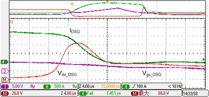 Figure 3-12 Short-Circuit Discharge Protection - MOSFET Off
The short circuit discharge protections are tested with the following processes:
- Both charge and discharge MOSFET are off with DET floating
- PACK port shorted together with air switch
- Turn on both charge and discharge MOSFET on with DET connected
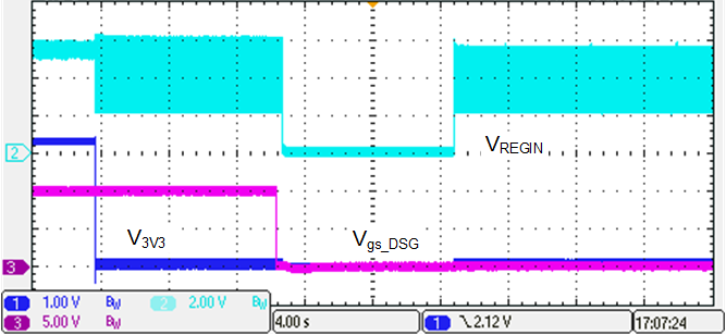 Figure 3-14 3.3-V Short and HWD Protections
When 3.3 V is shorted, the MCU is powered off and both BQ76942 devices detect HWD after some delay. Since TIDA-010247 configures MCU wake up from entering lower power mode (no communication with the BQ76942 to save power) every 5s, observe a range of 5s to 10s delay with 10s HWD delay configurations.
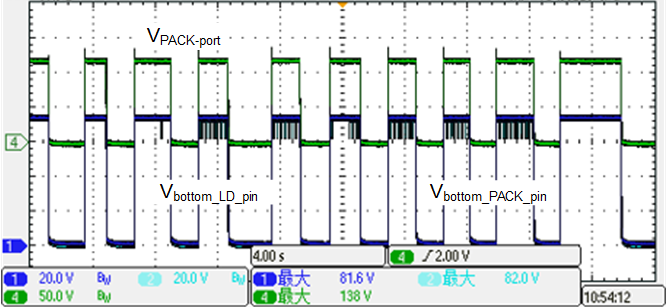 Figure 3-15 120 V On-PACK Port – Bottom AFE Maximum Voltage
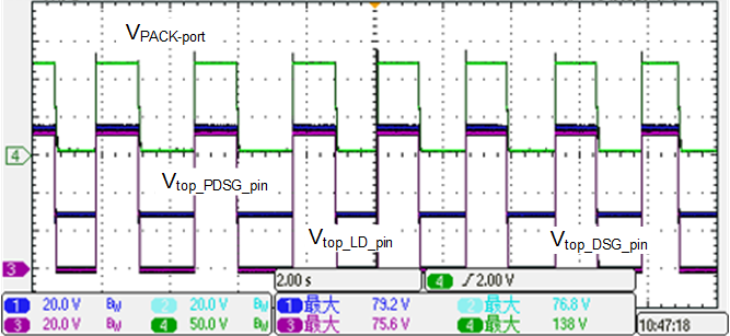 Figure 3-16 120 V On-PACK Port – Top AFE Maximum Voltage
The 120-V on PACK port test is carried out with both CHG and DSG MOSFET off with DET floating.