SBAA506 March 2021 ADS131B04-Q1 , ADS131M02 , ADS131M03 , ADS131M04 , ADS131M06 , ADS131M08
Component Selection
- The following table lists the
output voltage and current range for the INA821 and TLV171 amplifiers. These are
maximum overstress voltages and currents that may be applied to the ADS131M08
inputs. These input parameters should be limited to within the absolute maximum
ratings in step 2 to protect the ADS131M08 from damage.
INA821 Output Range TLV171 Output Range Output Voltage (VO) –5V ≤ VO ≤ +10V Output Voltage (VO) –5V ≤ VO ≤ +10V Short-circuit current (ISC) –20mA ≤ ISC ≤ +20mA Short-circuit current (ISC) –35mA ≤ ISC ≤ +25mA Since the specifications of the TLV171 are the worst case, all specifications from the TLV171 amplifier are used to design a protection circuit that works for both voltage (Vsense) and current (Isense) measurement channels on the ADS131M08.
The electrical overstress voltage from the ADS131M08 can reach up to the power supply of the TLV171, so the VEOS_MAX = +10V and the VEOS_MIN = –5V. The electrical overstress current from the ADS131M08 can be as high as the short-circuit current of the TLV171, so the I1_MAX = ISC_MAX = +25mA and the I1_MIN = ISC_MIN = –35mA.
- The input voltage range of the
ADS131M08 is set as the absolute maximum voltage (VIN_Abs ) before
turning on the internal ESD diode. The input current range of the ADS131M08 is
set as the absolute maximum current (IIN_Abs) that the internal ESD
diode can support continuously.
The following table, which comes from the absolute maximum ratings table in the ADS131M08 8-Channel, Simultaneously-Sampling, 24-Bit, Delta-Sigma ADC Data Sheet, shows that the absolute maximum input voltage on the ADS131M08 is 3.6V when AVDD is 3.3V, so any positive electrical overstress signal higher than 3.3V should be clamped to protect the ADS131M08 inputs. In this solution, the BAT54 Schottky diode is selected as D1 to protect the ADC from a positive electrical overstress signal because it has a small forward drop as well as reasonable low leakage and capacitance.
ADS131M08 Minimum (AGND = 0V) Maximum (AVDD = 3.3V) Absolute Maximum Ratings Analog Input Voltage (VIN_Abs) –1.6V
+3.6V Analog Input Voltage (IIN_Abs) –10mA +10mA - The current-limiting resistor,
R1, is selected as the larger resistor values between the R1_P,
calculated from the following equation for positive voltage overstress, and the R1_N,
calculated from the equation for negative voltage overstress.
- Positive overstress
voltage:
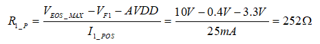
For a positive overstress voltage that is greater than +3.3V, the Schottky diode D1 operates in a forward state. The maximum input current in the circuit is +25mA from the TLV171. The forward voltage of D1 is around 0.4V at 25-mA forward current at 25°C based on the BAT54 data sheet from Diodes Incorporated. Therefore, VF1 = 0.4V and I1_POS = ISC_MAX = 25mA.
The required resistance of R1 under the positive overstress of +10V (R1_P) can be calculated as:
- Negative overstress
voltage:
The ADS131M08 has an integrated negative charge pump that allows operating for input voltages below ground (AGND) with a unipolar supply. When a negative overstress voltage lower than –1.44V is applied to the ADS131M08 input, the internal switch is turned on and the current (I2) flows into the ADC input as shown in the input current and voltage characteristics curve on the ADS131M08. The blue lines in the circuit show the current flow direction for a negative overstress voltage lower than –1.44V applied on the ADS131M08 input.
The minimum input voltage rating of the ADS131M08 (VIN_MIN) is –1.6V which is the minimum safe voltage to avoid damage to the device. Therefore, to achieve a minimum voltage signal of –1.6V on the ADC input pin (VIN), the node voltage, VD, should be equal to or greater than –1.6V. Two BAV199 diodes are used to clamp the negative overstress signal on VD with both diodes conducting in the forward direction. Hence, the forward voltage on each BAV199 diode is expected to be equal to or less than 0.8V. The D1 Schottky diode in the protection circuit operates in reverse state when a negative overstress signal appears. The leakage current on the D1 Schottky diode (BAT54) is only 2µA so the D1 diode is neglected in the following circuit.
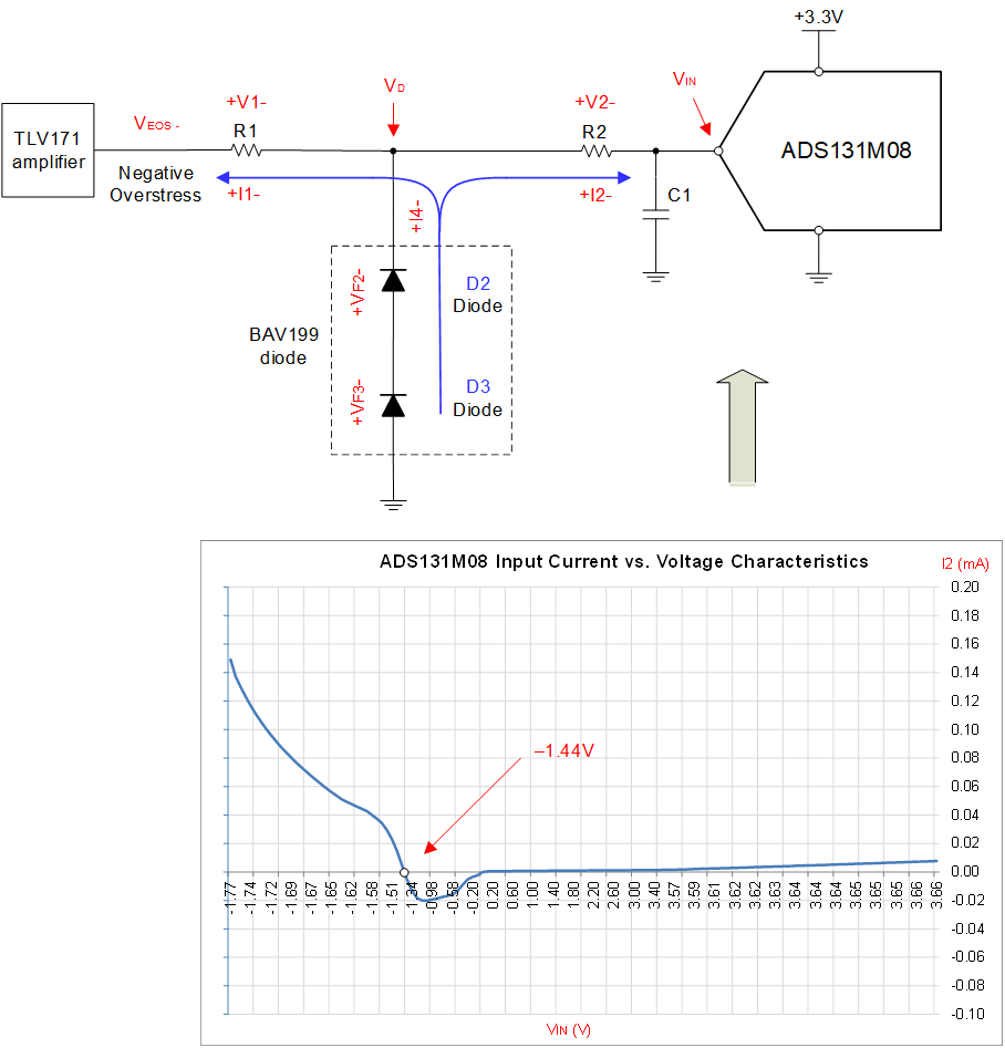
The forward current is found from the typical forward characteristics curve in the BAV199 data sheet from Diodes Incorporated. To limit the forward voltage of each diode on the BAV199 to 0.8V (VF2 = VF3 = 0.8V), the forward current (I4) needs to be limited to 4mA.
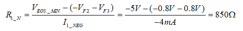
Since the VD is equal to VIN_MIN (–1.6V), the 4-mA current flows into the TLV171 amplifier and the current I1 under a negative overstress voltage of –5V (I1_NEG) is equal to –4mA. Therefore, the required resistance of R1 under a negative overstress of –5V (R1_N) can be calculated as:
The larger of the two resistance values from the previous equations is 850Ω. A large resistance is helpful to limit the electrical overstress current and clamp the electrical overstress voltage. Hence, R1 is selected as 1kΩ to account for extra design margin.
- Resistor Power Rating:
In the following equation, the fault current and power dissipated is calculated for R1 during a positive electrical overstress event which is the worse-case stress for R1.
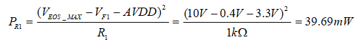
The objective is to make sure that the correct power rating is selected for R1.The minimum power rating for R1 is calculated to be 39.69mW according to the previous equation. A resistor with a 0.1-W power rating can be selected to account for extra design margin.
- Positive overstress
voltage:
- The resistor, R2, acts as a
low-pass filter with the capacitor C1 and also limits the current to the ADC
input under a fault condition. The value for R2 is selected as the larger
resistance between the R2_P, calculated from the equation for positive voltage overstress and R2_N,
calculated from the following equation for negative voltage overstress.
- Positive overstress
voltage:
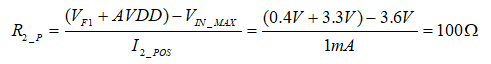
The absolute maximum input current rating (IIN_Abs) of the ADS131M08 is ±10mA. The smaller the input current flowing to the ADC inputs, the more reliably the circuit will perform. The ±1mA is used as the target maximum input current to the ADC to calculate for margin with one order of magnitude less than the absolute maximum ratings. Therefore, I2_POS = ±1mA. The forward voltage of D1 is around 0.4V at 25 mA forward current at 25°C based on the BAT54 data sheet from Diodes Incorporated. Therefore, VF1 = 0.4V. VIN_MAX = 3.6V which is the maximum absolute input voltage rating of the ADS131M08.
The required resistance of R2 under a positive overstresses voltage of +10V (R2_P) can be calculated as:
- Negative overstress
voltage:
Since the node voltage, VD, is designed to be equal to the VIN_MIN which is the minimum input voltage rating of the ADS131M08 (–1.6V) under a negative overstress voltage, very little current will flow into the ADC input. Therefore, the required resistance of R2 under a negative overstresses voltage of –5V (R2_N) is not critical.
The R2_P value is used to select R2 as the current into the ADC should be minimal during negative overstress conditions because the diodes (D2 and D3) limit the input voltage to avoid the overstress region. Therefore, R2 is selected as 100Ω.
- Resistor Power Rating:
In the following equation, the fault current and power dissipated is calculated in R2 during a positive electrical overstress event, which is the worse-case stress for R2. The objective is to make sure that the correct power rating is selected for R2. VF1 = 0.4V which is the forward voltage of BAT54 (D1) at 25-mA forward current at 25°C. VIN_MAX = 3.6V which is the maximum absolute input voltage rating of the ADS131M08.
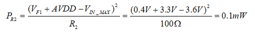
The minimum power rating for R1 is calculated to be 0.1mW according to the previous equation. A resistor with a 0.1-W power rating can be selected to account for extra design margin. The resistance of R2 can be adjusted to set the cutoff frequency of the filter as step 5 shows.
- Positive overstress
voltage:
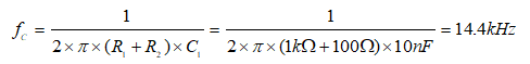
- The capacitor C1 in parallel with
R2 is used to filter the noise from the front-end circuit. The equation for the cutoff frequency based on the input resistors and
capacitors follows. The exact value may not be very critical so we use a
standard value of 10nF in the following formula.