SBAA506 March 2021 ADS131B04-Q1 , ADS131M02 , ADS131M03 , ADS131M04 , ADS131M06 , ADS131M08
AC (SNR and THD) Performance Checked on Hardware
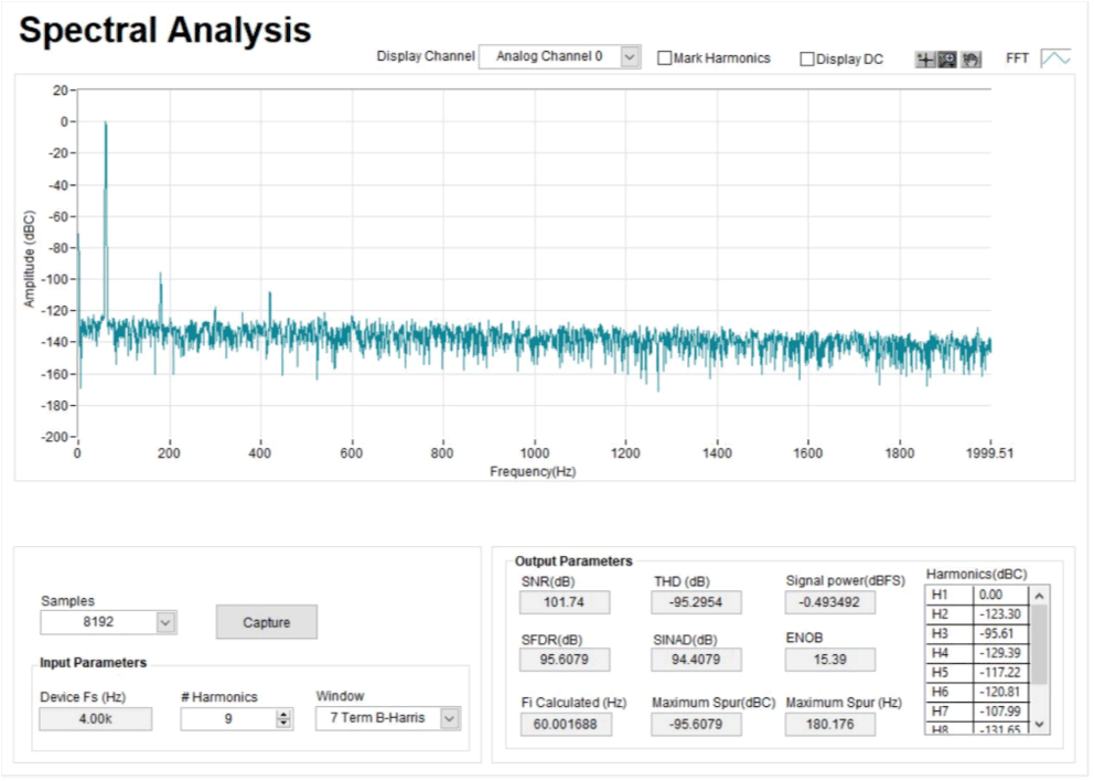
The following table shows the performance which is measured using ADS131M08EVM hardware with a schottky diode (BAT54) and dual-series Switching diode (BAV199) and the Delta-Sigma ADC Evaluation software.
| ADS131M08 | Specification in Data Sheet | Test 1 | Test 2 |
|---|---|---|---|
| SNR |
101 dB |
101.7 dB | 101.9 dB |
| THD |
–100 dB |
–95.3 dB | –95.2 dB |
- Test 1: R1 = 1kΩ, R2 = 100Ω with BAT54 (D1) and BAV199 (D2 and D3).
- Test 2: R1 = 1kΩ, R2 = 100Ω without BAT54 (D1) and BAV199 (D2 and D3).
- Protection: a same protection circuit is designed on AINxP and AINxN input of ADS131M08 and a differential capacitor is applied between the AINxP and AINxN input.
- Test signal: a differential sinusoidal wave with 60-Hz frequency and –0.5dBFS amplitude, 4-kSPS data rate, Gain = 1, OSR = 1024 and internal voltage reference.
The measured SNR performance with all the protection circuits including the BAT54 and BAV199 diode meets the typical specification in the ADS131M08 8-Channel, Simultaneously-Sampling, 24-Bit, Delta-Sigma ADC Data Sheet. The measured THD performance is worse than the typical THD specification in the ADS131M08 data sheet. An additional test (Test 2) shows that the slightly worse THD performance in Test 1 is not caused by the protection diodes and it is caused by the combination between the large resistance of these two series (R1 and R2) and the parameter of ADC input structure that varies with the voltage applied on the ADC input. The following figure shows the measured spectral analysis in Test 1.