SBAA506 March 2021 ADS131B04-Q1 , ADS131M02 , ADS131M03 , ADS131M04 , ADS131M06 , ADS131M08
ADC Input Overvoltage Condition
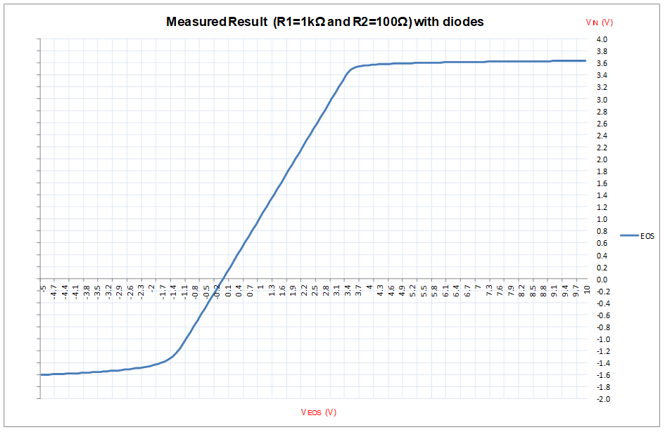
The following figure shows the voltage (VIN) measured on the ADC input with a multimeter when a continuous overstress signal (VEOS) is applied from –5V to +10V. Note that the external BAT54 Schottky diode (D1) is turned on for positive overvoltage signals and the external BAV199 dual series switching diodes (D2 and D3) are turned on for negative overvoltage signals. The overstress signals have been clamped to approximate +3.6V and –1.6V, which is equal to the absolute maximum input voltage ratings (VIN_Abs) on the ADS131M08, so the ADC is successfully protected from external overvoltage event.