SBAA507 March 2021 ADS8578S , ADS8584S , ADS8586S , ADS8588H , ADS8588S , ADS8598H , ADS8598S , ADS8661 , ADS8664 , ADS8665 , ADS8668 , ADS8671 , ADS8674 , ADS8675 , ADS8678 , ADS8681 , ADS8684 , ADS8684A , ADS8685 , ADS8688 , ADS8688A , ADS8688AT , ADS8689 , ADS8691 , ADS8694 , ADS8695 , ADS8698 , ADS8699 , OPA2990 , OPA4990 , OPA990
Component Selection
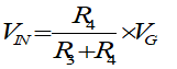
- The normal input signal range (VG) is
±12.88V. VG is scaled down by the resistor divider (R3 and R4) to
provide margin above the normal input voltage range for the floating input
detection voltage. The following table lists the input range on the ADS8681 in this design, the input voltage range (VG), and
the expected normal voltage (VIN) on the ADC input for 1-V
margin.
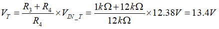
Input Signal Voltage (VG) ADS8681 Input Range (VADC) Expected Normal Voltage on ADC Input (VIN) Expected Voltage on ADC Input for Float (VIN_T) Maximum +12.88V +12.88V +11.88V +12.38V Minimum –12.88V –12.88V –11.88V +12.38V R3 is selected as 1kΩ for a small gain and offset error. Therefore, R4 is determined by the following equation:
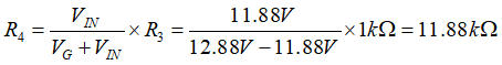
A 12-kΩ and 0.1% tolerance resistor is finally selected for R4. The resistor value can be adjusted according to the noise and margin required in the system.
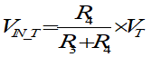
- The objective of this step is to select the ADC
input voltage under which a float is detected (called VIN_T). This
voltage is selected to be 0.5V higher than the highest normal operating input
voltage (+11.88V) for margin to prevent a false detection of a float condition.
Therefore, the VIN_T can be calculated from the equation:

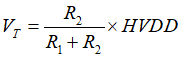
- The objective of this step is to select a voltage divider on the input of the amplifier (OPA990) that will set the float voltage at the input of the ADC as
selected in step 2. VIN_T is the divided input down threshold voltage
(VT) during a floating input condition. Use the following equations to calculate the required VT voltage to achieve the
desired VIN_T:
R1 and R2 are selected to create the VT voltage during floating inputs. To achieve higher input impedance, R2 is selected as 10MΩ. R1 is determined by the following equation:
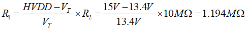
R1 is selected as 1.2MΩ which is a standard resistor value. Note that the tolerance on these resistors only impacts the float voltage accuracy.
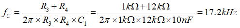
- The capacitor C1 in parallel with R3||R4 is used to filter the noise from the front-end circuit.
The equation for the cutoff frequency based on the input resistors and
capacitors follows. The exact value may not be critical so we use a standard
value of 10nF in this design.