SBAA507 March 2021 ADS8578S , ADS8584S , ADS8586S , ADS8588H , ADS8588S , ADS8598H , ADS8598S , ADS8661 , ADS8664 , ADS8665 , ADS8668 , ADS8671 , ADS8674 , ADS8675 , ADS8678 , ADS8681 , ADS8684 , ADS8684A , ADS8685 , ADS8688 , ADS8688A , ADS8688AT , ADS8689 , ADS8691 , ADS8694 , ADS8695 , ADS8698 , ADS8699 , OPA2990 , OPA4990 , OPA990
Simulation Verification for Floating Input
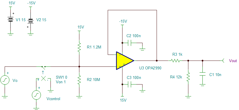
The following circuit is used in TINA-TI to simulate and verify if the output voltage is correct as expected when the input of amplifier is floating. A voltage-controlled switch (SW1) is intentionally added to simulate the connection and disconnection status. The switch (SW1) is controlled by a periodic voltage signal (Vcontrol) for open and close.
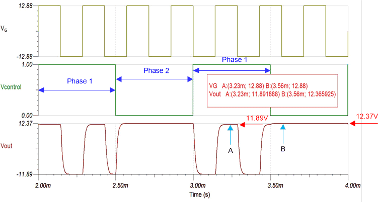
The simulated result is shown in the following graph. The continuous input signal (VG) sweeps within the normal voltage range of ±12.88V. The control signal (Vcontrol) forces the switch (SW1) to turn on for a connected state in phase 1. The simulation shows a ±11.89-V output signal (Vout) in phase 1. The control signal (Vcontrol) forces the switch (SW1) to turn off for a floating state in phase 2. The simulation shows a 12.37-V output signal (Vout) in phase 2. Note that the simulated value and calculated value (12.38V) match well.