SBAA515A June 2021 – September 2022 AMC3301 , AMC3301-Q1 , AMC3302 , AMC3302-Q1 , AMC3306M05 , AMC3306M25 , AMC3330 , AMC3330-Q1 , AMC3336 , AMC3336-Q1
4.1 Device Orientation
As mentioned previously, the coils of the internal DC/DC converter have a parasitic capacitance from the primary side to the secondary side of the isolation barrier, and the energy radiates from the device pins, and traces connected to pins. As a result, it is important to consider how the AMC3301 family will radiate and affect other devices along the isolation barrier, including other AMC3301’s.
 Figure 4-1 Device orientation examples
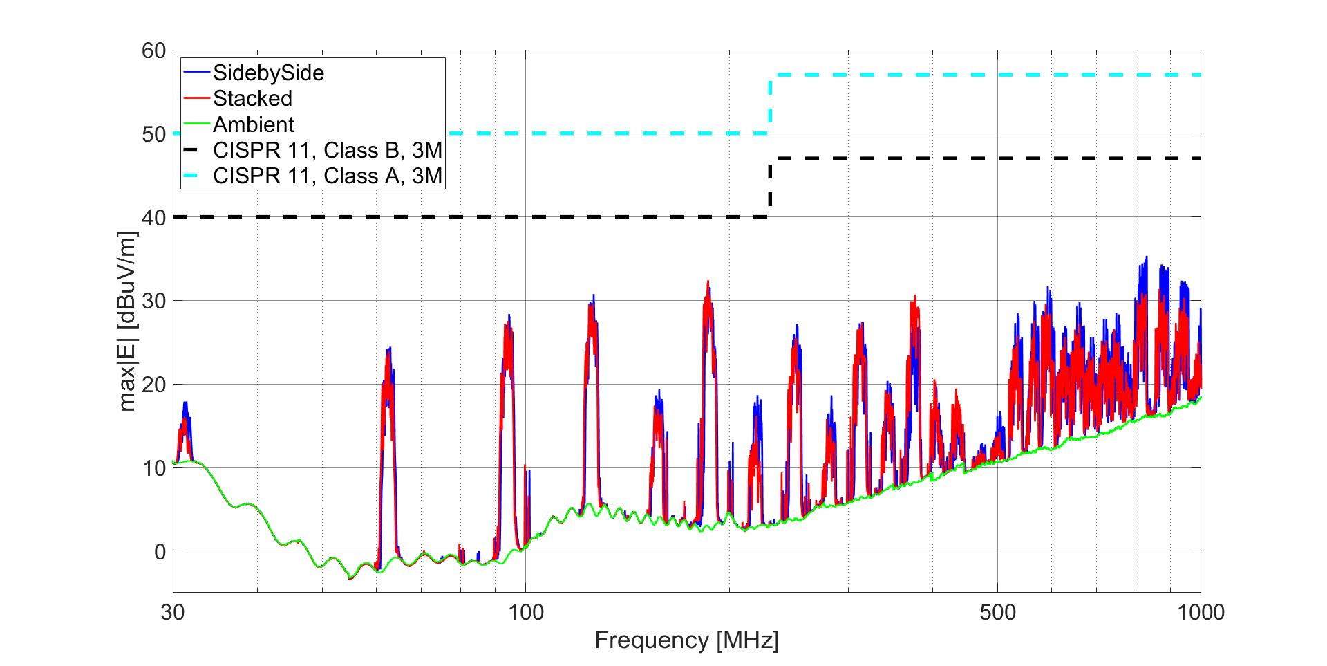
To demonstrate the effects of device orientation, a stacked orientation and side-by-side orientation are tested. The schematic used in testing is the same as the ferrite section of Figure 4-1. The input ferrite beads part number is 74269244182, and they were tested with 1.5 m input shorted together.
Figure 4-2 shows the orientations will meet the CISPR 11 class B limit as a result of the ferrite beads discussed previously. The stacked orientation is in red while the side-by-side orientation is in blue. In addition, the orientations fall within 5 dBuV/m of each other. However, placing both devices right on top of each other-in a stacked orientation-shows the best performance.
 Figure 4-2 Multiple AMC3301 CISPR 11 Measurements with 1.5 m Input