SBAU230C August   2014  – March 2021 ADS8688


  1. Trademarks
  2. ADS8688EVM-PDK Overview
  3. EVM Analog Interface
    1. 3.1 ADC Analog Input Connections and Filter
    2. 3.2 Voltage Reference, Aux Input, and Supply Decoupling
  4. Digital Interface
    1. 4.1 Serial Interface (SPI)
    2. 4.2 I2C Bus for Onboard EEPROM
  5. Power Supplies
  6. ADS8688 Initial Setup
    1. 6.1 Software Installation
  7. EVM Operation
    1. 7.1 Connecting the Hardware
    2. 7.2 Modifying Hardware and Using Software to Evaluate Other Devices in the Family
    3. 7.3 EVM GUI Global Settings for ADC Control
    4. 7.4 Time Domain Display
    5. 7.5 Frequency Domain Display
    6. 7.6 Histogram Display
  8. Bill of Materials, Schematics, and Layout
    1. 8.1 Bill of Materials
    2. 8.2 Board Layout
    3. 8.3 Schematic
  9. 10Revision History

Board Layout

Figure 8-1 shows the PCB layout for the ADS8688EVM.

Note:

The board layouts is not to scale. This figure is intended to show how the board is laid out and is not intended to be used for manufacturing ADS8688EVM PCBs.
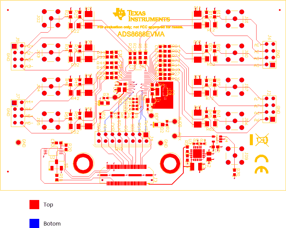
GUID-20210312-CA0I-6KBJ-NGGB-JHMKQWT3GT2W-low.gifFigure 8-1 ADS8688EVM PCB