SBAU382A November 2021 – January 2022 ADS7029-Q1 , ADS7039-Q1 , ADS7040 , ADS7041 , ADS7042 , ADS7043 , ADS7044 , ADS7046 , ADS7047 , ADS7049-Q1 , ADS7052 , ADS7054 , ADS7056 , ADS7057
2.4 I2C Bus for Onboard EEPROM
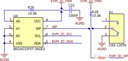
The circuit shown in Figure 2-8 is used with the PHI board to identify the specific ADCs populated on the EVM and enable the correct GUI settings. The user does not need to modify or interact with this circuit during EVM operation. As a result, switch S1 is set by default to enable the EEPROM write protect and must not be altered unless the ADC is modified as per Section 2.1.1 or Section 2.1.2. Update the EEPROM when the ADC is replaced using the ADS704X-5XEVM GUI, as per Section 4.6.
 Figure 2-8 EEPROM Circuit on the ADS704X-5XEVM