SBOA447 November 2020 ALM2402-Q1 , ALM2402F-Q1 , ALM2403-Q1
2 ALM2402F-Q1 Output Fault Protection
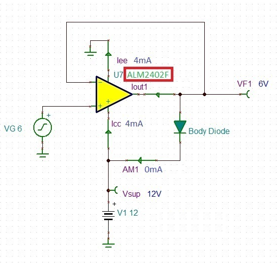
Figure 2-1 shows the ALM2402F-Q1 under normal quiescent condition being powered from 12 V single supply with its input and output voltage at 6 V mid-supply (no fault condition).
 Figure 2-1 ALM2402F-Q1 Normal
Operation
Figure 2-1 ALM2402F-Q1 Normal
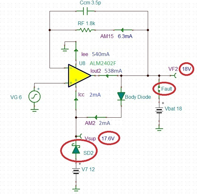
OperationFigure 2-2 shows ALM2402F-Q1 under a fault condition with its output being shorted to an 18 V battery while being powered by a 12 V supply, requiring only protection of a blocking Schottky diode, SD2. Since the absolute maximum rated supply voltage for ALM2402F-Q1 is 18 V, adding the blocking diode, SD2, allows the battery voltage, Vbat, to pull up the amplifier’s positive supply pin, Vsup, to 17.6 V without any damage.
 Figure 2-2 ALM2402F-Q1 18 V Battery Fault
Protection
Figure 2-2 ALM2402F-Q1 18 V Battery Fault
ProtectionThe addition of 1.8kΩ resistor in the feedback, RF, shown in Figure 2-2, limits to 10mA maximum allowable current through the internal back-to-back input protection diodes located between the ALM2402F-Q1 input terminals.
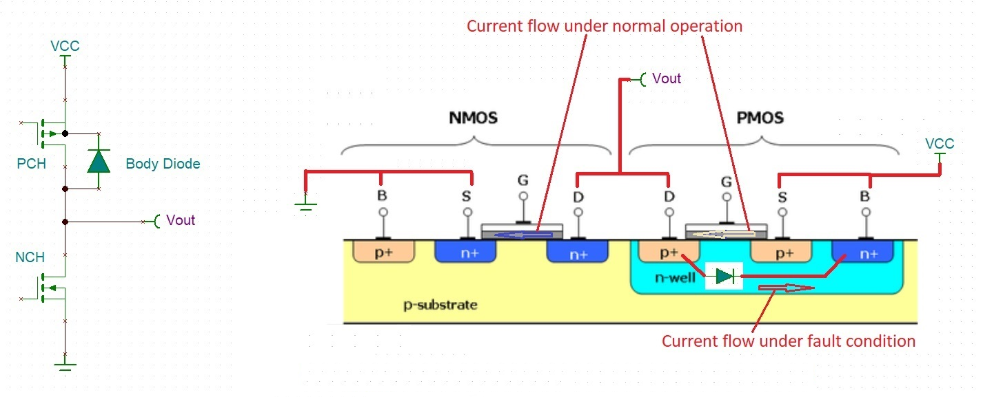
Under the short to battery conditions output of ALM2402F-Q1 sinks 538mA short-circuit current (see Figure 2-2) attempting to bring down the output voltage. At the same time a body diode - an internal drain-to-nwell, p-n junction of P-channel output transistor - supplies 2mA quiescent current to bias the first two internal stages of the amplifier. Under normal operation of the output PMOS transistor, the current flows through the enhanced p-channel from Vcc to Vout. However, under the fault conditions, when Vout is above Vcc, normal operation of PMOS is shut down (Vgs=0) and thus the current flows in a reverse direction from the output, Vout, through drain-to-nwell body diode to a positive supply – see Figure 2-3. For this reason, under fault condition Vsup gets pulled up within a diode drop below Vbat voltage (see Figure 2-2).
 Figure 2-3 Normal vs. Fault Operation of
the Output Stage