SBOA585 March 2024 ADS127L11 , ADS127L11 , ADS127L14 , ADS127L14 , ADS127L18 , ADS127L18 , ADS127L21 , ADS127L21 , PGA849 , PGA849 , PGA855 , PGA855
- 1
- Abstract
- Trademarks
- 1PGA855 and ADS127L21, 24-Bit, Delta-Sigma ADC Driver Circuit
- 2PGA855 Analog Front-End Filters
- 3ADS127Lx1 Delta-Sigma ADC and Digital Filter
- 4Approximate PGA855 Intrinsic Noise Analysis
- 5PGA855 and ADS127Lx1 System Noise
- 6PGA855 and ADS127Lx1 SNR and Noise Calculator
- 7PGA855 and ADS127Lx1 FFT Measured Performance
- 8Summary
- 9References
2 PGA855 Analog Front-End Filters
The PGA855 analog-front-end circuit consists of three analog filters. Figure 7-13 shows the filters of the PGA855-ADS127Lx1 circuit.
 Figure 2-1 PGA855 Analog Filters
The first analog filter located at the input of the PGA helps reduce electromagnetic interference (EMI) and radio frequency interference (RFI) high-frequency extrinsic noise. This input filter can be customized per the application bandwidth and anti-aliasing requirements.
This circuit example uses a filter with the capacitor ratio of CIN_DIFF = 10 × CIN_CM. Using the 10-to-1 ratio for differential capacitor CIN_DIFF versus common-mode capacitors CIN_CM offers good differential and common-mode noise rejection. This ratio of capacitor values also tends to be less sensitive to the tolerance variation and mismatch of the filter capacitors. When the CIN_DIFF capacitor value is chosen to be 10 times larger than the common-mode capacitors, the resulting differential filter provides a corner frequency that is 20 times lower than the common-mode filter corner frequency. Therefore, differential signals are attenuated at a lower frequency than the common-mode signals. The instrumentation amplifier amplifies differential signals and rejects the common-mode voltage signals. Providing this ratio of capacitors helps to mitigate the effects due to the mismatch of the common-mode capacitors, where the asymmetric noise attenuation caused by the common-mode capacitor mismatch is attenuated to insignificant levels. By simple inspection, derive Equation 1 and Equation 2 to calculate the corner frequencies:
EMI/RFI input filter differential-mode corner frequency:
EMI/RFI input filter common-mode corner frequency:
Equation 1 provides an input differential filter f-3dB corner frequency of 7.58MHz. When measuring bridge sensors with high-resistance, the sensor resistance can affect the corner frequency of the input filter.
The second filter helps to limit the PGA855 intrinsic noise contribution, and works as a low-pass anti-aliasing filter. Typically, the bandwidth of the feedback filter can be adjusted per the application bandwidth requirements. This filter is implemented with the feedback capacitor, CFB, in parallel with the PGA855 output-stage 5kΩ feedback resistors forming a 1st order filter.
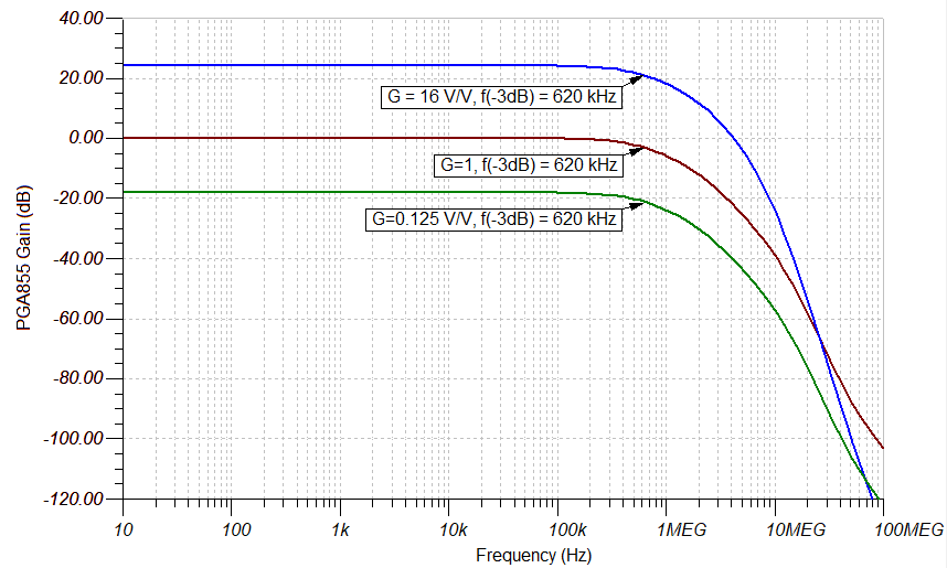
The PGA855 circuit bandwidth is limited by CFB. In this example, CFB is set to 47pF, in parallel with the output-stage 5kΩ feedback resistor providing a typical f–3dB corner frequency of 677kHz.
Note that the PGA855 internal fully differential amplifier output stage resistors, although precisely ratio-metrically matched among each other to provide very low gain error, can exhibit a ±15% absolute resistance over process and temperature variation, and this resistor variation must be taken in to account when implementing the noise filtering. The f–3dB corner frequency for the feedback filter can vary in the range of approximately 589kHz to approximately 677kHz when accounting for the 5kΩ ±15% absolute resistance variation of the internal feedback resistors.
The third differential R-C-R filter at the ADS127Lx1 inputs serves two purposes. First, the filter provides a third pole to the overall filter response, thereby increasing the filter rolloff slope. The filter also works as a charge reservoir to filter the sampled input of the ADC. The charge reservoir reduces the instantaneous charge demand of the amplifier, maintaining low distortion and low gain error that otherwise can degrade because of incomplete amplifier settling. The ADC input filter values are RFIL = 47.4Ω, CDIFF = 560pF, and CCM = 51pF. The ADS127Lx1 input precharge buffers significantly reduce the sample-and-hold input charge that raises the ADC input impedance to decrease gain error.
High-grade C0G (NP0) are used everywhere in the signal path (CIN_DIFF, CIN_CM, CFB, CDIFF, CCM) for low distortion. Among ceramic surface-mount capacitors, the type of dielectric used in C0G (NP0) capacitors provides the most stable electrical properties over voltage, frequency, and temperature changes.
The PGA855 analog front-end circuit, accounting for all three analog filters, provides a nominal f–3dB bandwidth of 620kHz. On the high side of the internal 5kΩ feedback resistor tolerance, the PGA855 f–3dB bandwidth changes to 547kHz and the circuit maintains –0.1dB flatness to 85kHz. Figure 2-2 shows the TINA-TI simulated PGA855 AC frequency response.
 Figure 2-2 PGA855 Frequency Response Simulation Result