SBVA067A December 2019 – September 2020 TLV733P-Q1
4.1 WSON-6 Package
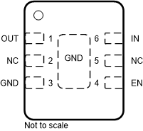
Figure 4-1 shows the TLV733P-Q1 pin diagram for the WSON-6 package. For a detailed description of the device pins please refer to the Pin Configuration and Functions section in the TLV733P-Q1 data sheet.

Figure 4-1 Pin Diagram (WSON-6) Package
Table 4-2 Pin FMA for Device Pins
Short-Circuited to Ground
| Pin Name | Pin No. | Description of Potential Failure Effect(s) | Failure Effect Class |
|---|---|---|---|
| OUT | 1 | Output voltage will be near/at ground. Device is in current limit. It may cycle in and out of thermal shutdown depending on power dissipation. | B |
| NC | 2 | Normal operation. | D |
| GND | 3 | Normal operation. | D |
| EN | 4 | LDO will not start up due to EN being grounded. | B |
| NC | 5 | Normal operation. | D |
| IN | 6 | Output voltage will be near/at ground. | B |
Table 4-3 Pin FMA for Device Pins
Open-Circuited
| Pin Name | Pin No. | Description of Potential Failure Effect(s) | Failure Effect Class |
|---|---|---|---|
| OUT | 1 | No impact to the LDO, but components downstream will not be powered. | D |
| NC | 2 | Normal operation. | D |
| GND | 3 | GND is floating. Output voltage will be incorrect as it is no longer referenced to GND. | B |
| EN | 4 | EN pin voltage will float as the LDO contains no internal pullup/pulldown. LDO is in unknown state. | B |
| NC | 5 | Normal operation. | D |
| IN | 6 | No input to LDO. Input and output will float to an unknown voltage. | B |
Table 4-4 Pin FMA for Device Pins
Short-Circuited to Adjacent Pin
| Pin Name | Pin No. | Shorted to | Description of Potential Failure Effect(s) | Failure Effect Class |
|---|---|---|---|---|
| OUT | 1 | 2 - NC | Normal operation. | D |
| NC | 2 | 3 - GND | Normal operation. | D |
| GND | 3 | 4 - EN | LDO will not start up due to EN being grounded. | B |
| EN | 4 | 5 - NC | Normal operation. | D |
| NC | 5 | 6 - IN | Normal operation. | D |
| IN | 6 | 1 - OUT | No output voltage regulation. Output voltage is the same as input voltage. | B |
Table 4-5 Pin FMA for Device Pins Short-Circuited to
VIN
| Pin Name | Pin No. | Description of Potential Failure Effect(s) | Failure Effect Class |
|---|---|---|---|
| OUT | 1 | No output voltage regulation. Output voltage is the same as input voltage. | B |
| NC | 2 | Normal operation. | D |
| GND | 3 | Output voltage will be near/at ground. | B |
| EN | 4 | LDO will startup/shutdown when VIN is above EN threshold. | D if VIN = VEN by design, B otherwise |
| NC | 5 | Normal operation. | D |
| IN | 6 | Normal operation. | D |