SBVU076 April 2022
2.3 TPS7A74 LDO Operation and Component Selection
The TPS7A74EVM-068 evaluation module contains the TPS7A74 LDO with input, bias, soft-start, and output capacitors installed, as well as feedback resistors installed. These seven components provide an implementation example, as illustrated by the white boxes in Figure 2-2. The prepopulated capacitors are sized to ensure the minimum capacitance requirements are maintained under all normal operating conditions. Optional pads are available to test the LDO with additional setpoint options, as well as input, bias, and output capacitors beyond what is already installed on the EVM.
Setpoint resistors are prepopulated on the TPS7A74EVM-068 to provide an output voltage of 1 V, 1.2 V, 1.5 V, 1.8 V, or 3.3 V. Select one of these output voltages by using the provided shunt to short the necessary pin on header J16. If 0.65 V is desired on VOUT, remove the shunt from J16 and short J6. For other voltage options, resistor R10 can be populated and R1 modified as necessary. See the Application and Implementation section in the TPS7A74 data sheet for guidance on selecting R10 and R1 for alternate values of VOUT.
The TPS7A74 LDO can be enabled or disabled by using the J9 3-pin header:
- Place a 2-pin shunt across the header to tie VIN to EN to enable the device
- Place a 2-pin shunt across the header to tie GND to EN to disable the device
Alternatively, by connecting an external function generator to TP1 (EN) and a nearby GND post (J17), the user can enable or disable the TPS7A74 LDO after VIN is applied. Figure 2-1 illustrates the result of the TPS7A74EVM-068 during turn-on. The blue trace is the enable voltage, the green trace is the output voltage, and the red trace is the load current.
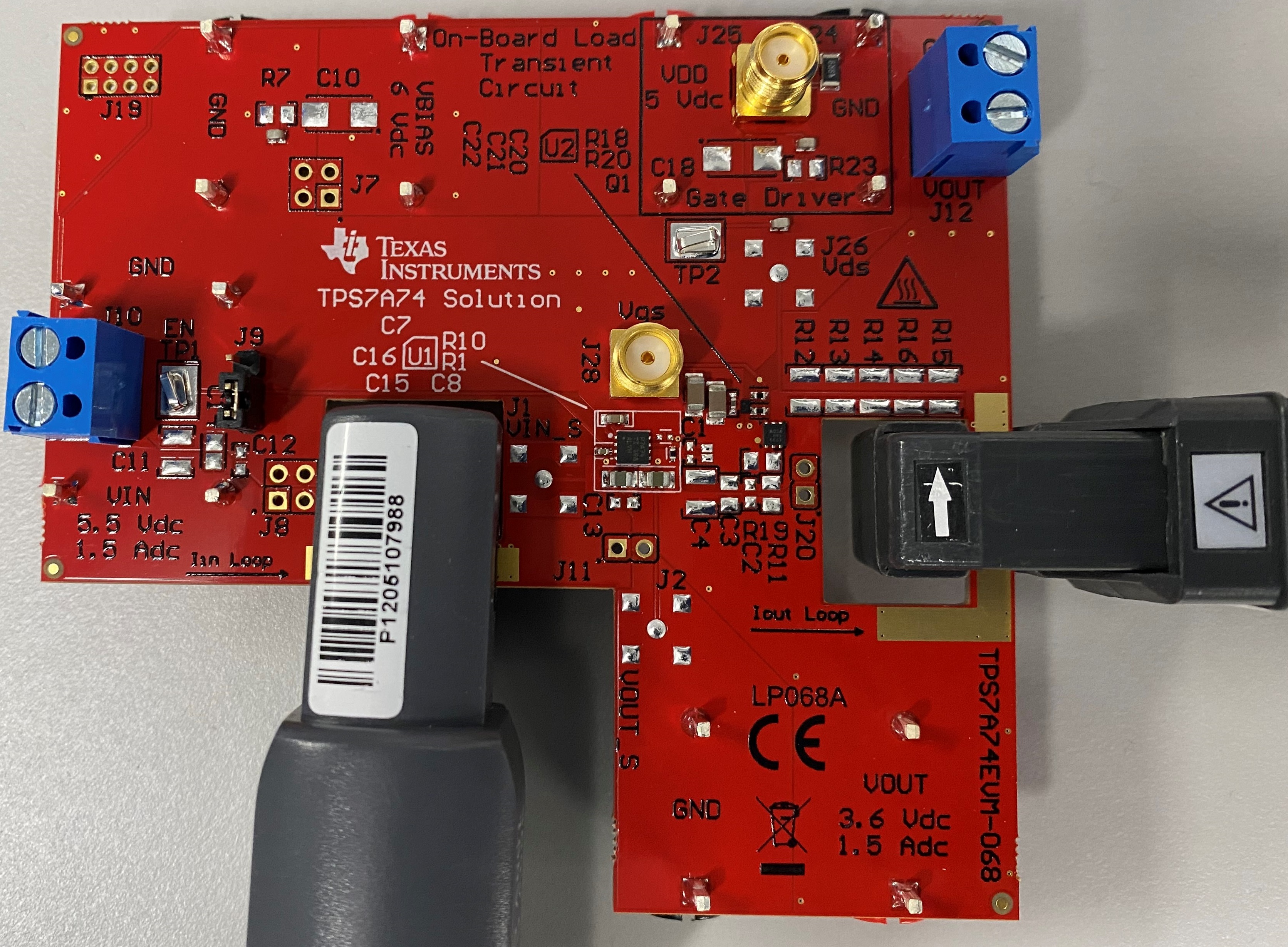
If desired, a current probe can be inserted in the EVM as shown in Figure 2-2 to measure the input and output current. The slots were sized to fit most current probes, such as the LeCroy™ AP015 or CP031 current probes.
 Figure 2-2 TPS7A74EVM-068 With Current
Probes Attached
Figure 2-2 TPS7A74EVM-068 With Current
Probes AttachedThe user has two options for providing a DC load on the output of the TPS7A74. J12 can be used to place a DC load that flows through the current sense path on the output of the LDO. Alternatively, the J4 (VOUT) and J18 (GND) banana connectors can be used for external measurements and loading; however, the IOUT loop does not sense current flowing through these connectors. In cases where very fast transient tests are performed, ringing may occur on VIN or VOUT as a result of the PCB parasitic inductance. Placing a strip of wire on the exposed copper in the current path can reduce this ringing. 10 AWG wire can be used as needed. If ringing persists, install damping networks by adding a series resistor and capacitor in parallel with VIN. Locations where damping can be installed include C5 and R8, C6 and R9, C10 and R7, and C18 and R23.
Optional kelvin sense points are provided using the SMA connectors J1 (VIN) and J2 (VOUT).