SBVU078 November   2022


  1.   Abstract
  2.   Trademarks
  3. 1Introduction
  4. 2Setup
    1. 2.1 LDO Input/Output Connector Descriptions
      1. 2.1.1 VIN and GND
      2. 2.1.2 BIAS and GND
      3. 2.1.3 VOUT and GND
      4. 2.1.4 EN
    2. 2.2 Optional Load Transient Input/Output Connector Descriptions
      1. 2.2.1 VDD and GND
      2. 2.2.2 J16
      3. 2.2.3 J18
      4. 2.2.4 J21
      5. 2.2.5 J22
      6. 2.2.6 J23
      7. 2.2.7 J24
    3. 2.3 TPS7A53A-Q1 LDO Operation and Component Selection
    4. 2.4 Optional Load Transient Circuit Operation
  5. 3Board Layout
  6. 4TPS7A53EVM-080 Schematic
  7. 5Bill of Materials

TPS7A53EVM-080 Schematic

Figure 4-1 shows a schematic for the TPS7A53EVM-080.
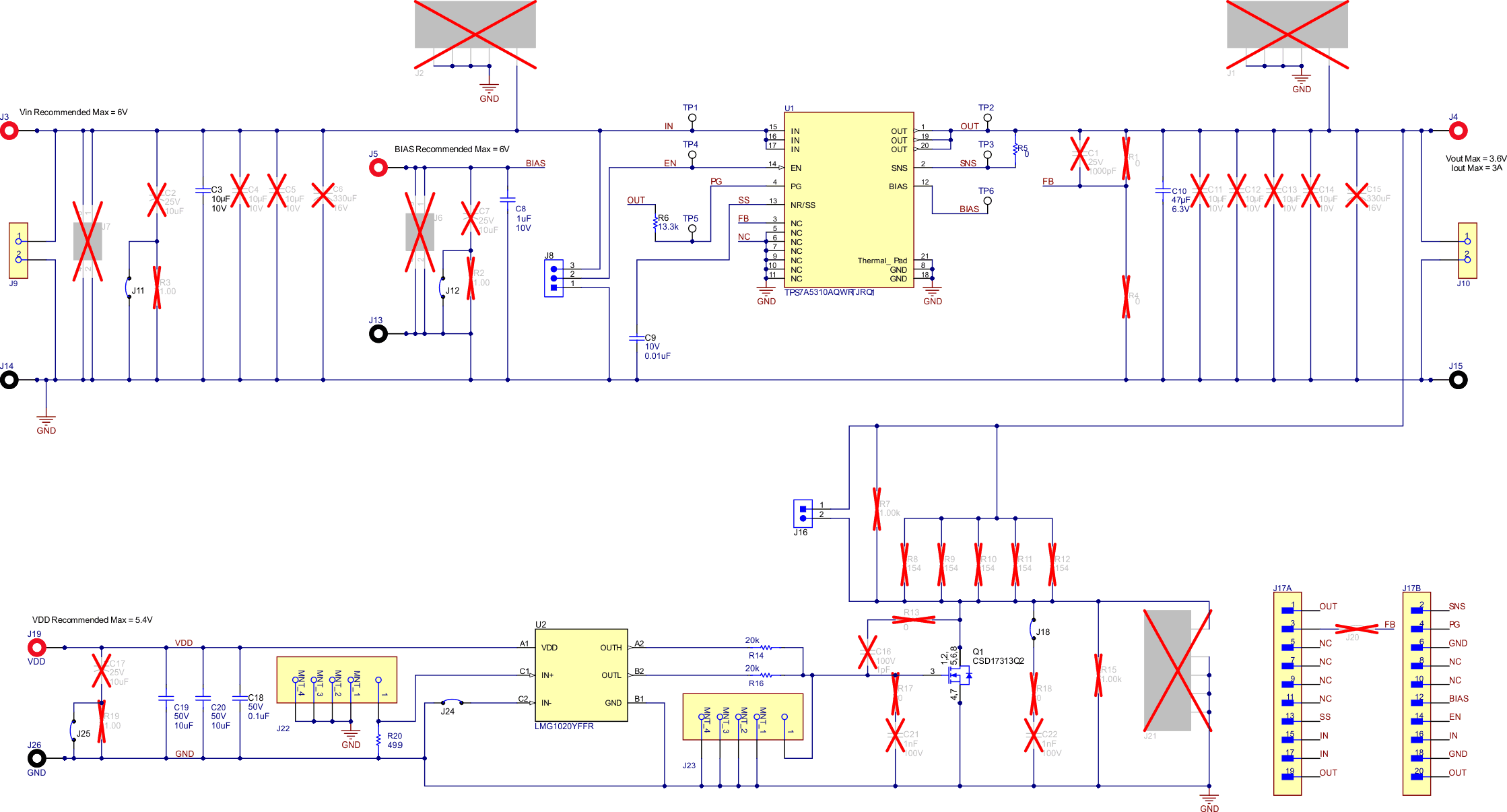
GUID-20220921-SS0I-BXVC-ZH6G-ZCB4NWKRZCLH-low.gifFigure 4-1 Schematic