SBVU078 November 2022
- Abstract
- Trademarks
- 1Introduction
- 2Setup
- 3Board Layout
- 4TPS7A53EVM-080 Schematic
- 5Bill of Materials
3 Board Layout
Figure 3-1 through Figure 3-8 illustrate the board layout for the TPS7A53EVM-080 PCB.
The TPS7A53EVM-080 dissipates power, which can cause some components to experience an increase in temperature. The TPS7A53A-Q1 LDO and pulsed resistors R8, R9, R10, R11, and R12 are most at risk of raising the junction temperature during normal operation. The LDO can become hot to the touch during normal operation, see the thermal impedance discussion in the TPS7A53A-Q1 data sheet.
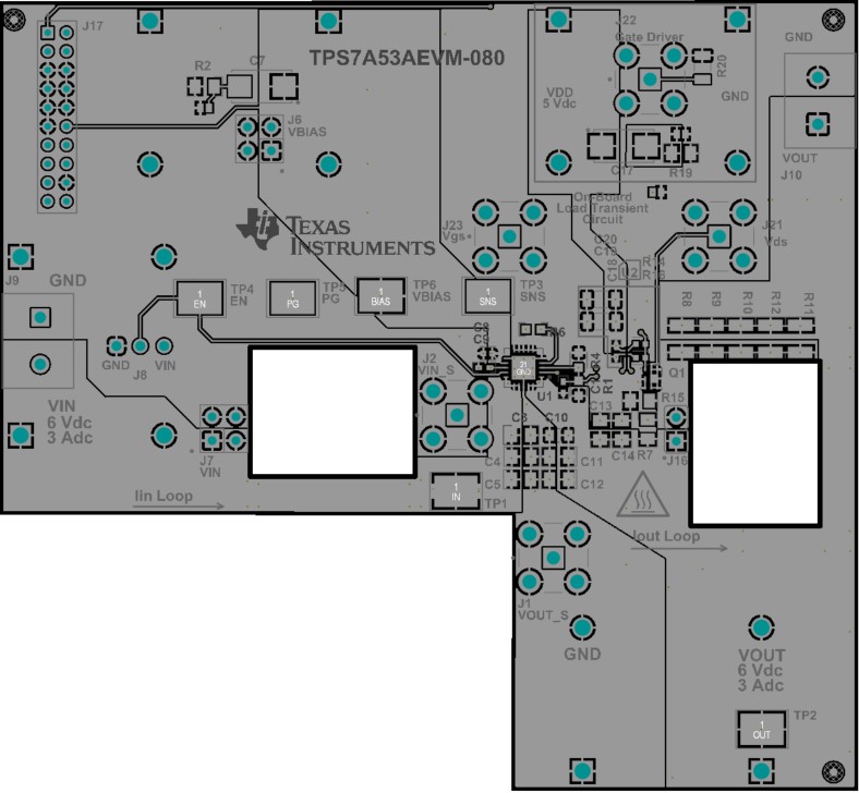 Figure 3-1 Top Assembly Layer and
Silkscreen
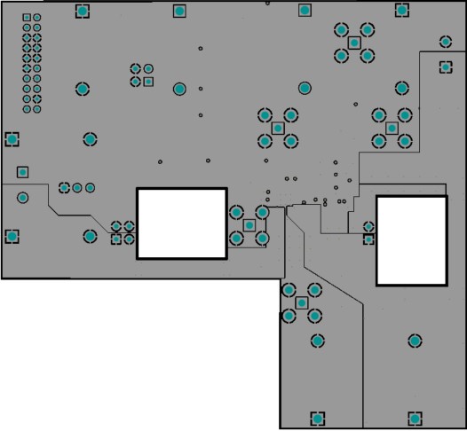 Figure 3-3 Layer 2
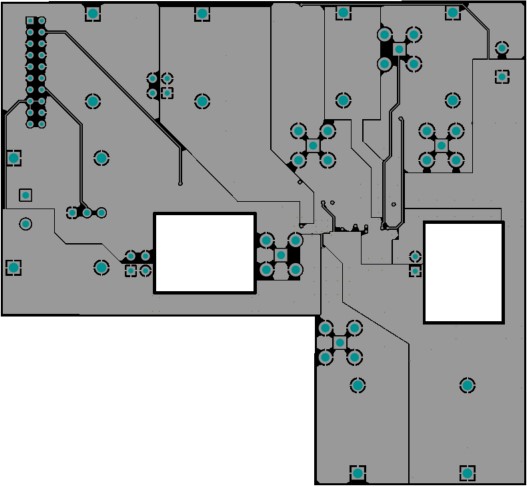 Figure 3-5 Layer 4
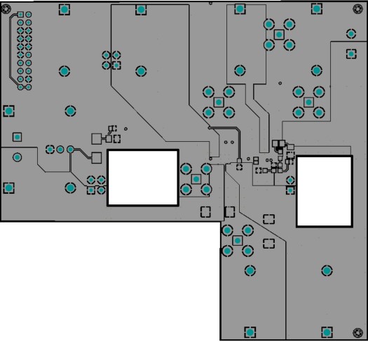 Figure 3-7 Bottom Layer
Routing
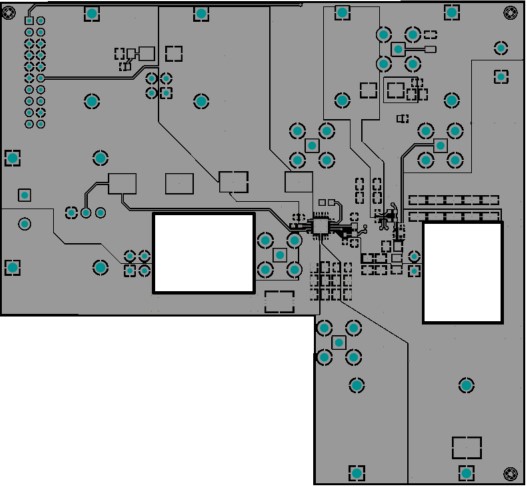 Figure 3-2 Top Layer Routing
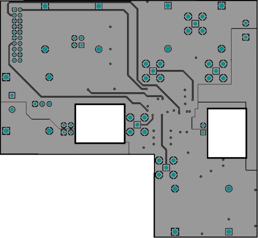 Figure 3-4 Layer 3
 Figure 3-6 Layer 5
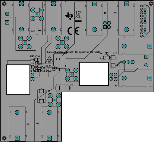 Figure 3-8 Bottom Assembly Layer and
Silkscreen