SLAA919A October 2019 – March 2020 MSP430FR2310 , MSP430FR2311 , MSP430FR2353 , MSP430FR2355
Design Goals
| Input ViDiff (Vi2 – Vi1) | Output | Supply | ||||
|---|---|---|---|---|---|---|
| ViDiff_Min | ViDiff_Max | VoMin | VoMax | Vcc | Vee | Vref |
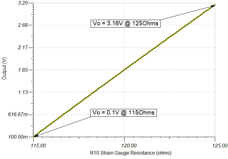
| –2.22 mV | 2.27 mV | 0.1 V | 3.2 V | 3.3 V | 0 V | 1.65 V |
| Strain Gauge Resistance Variation (R10) | Vcm | Gain |
|---|---|---|
| 115 Ω to 125 Ω | 1.34 V | 690 V/V |
Design Description
Some MSP430™ microcontrollers (MCUs) contain configurable integrated signal chain elements such as op-amps, DACs, and programmable gain stages. These elements make up a peripheral called the Smart Analog Combo (SAC). For information on the different types of SACs and how to leverage their configurable analog signal chain capabilities, visit MSP430 MCUs Smart Analog Combo Training. To get started with your design, download the Strain Gauge Bridge Amplifier Circuit Design Files.
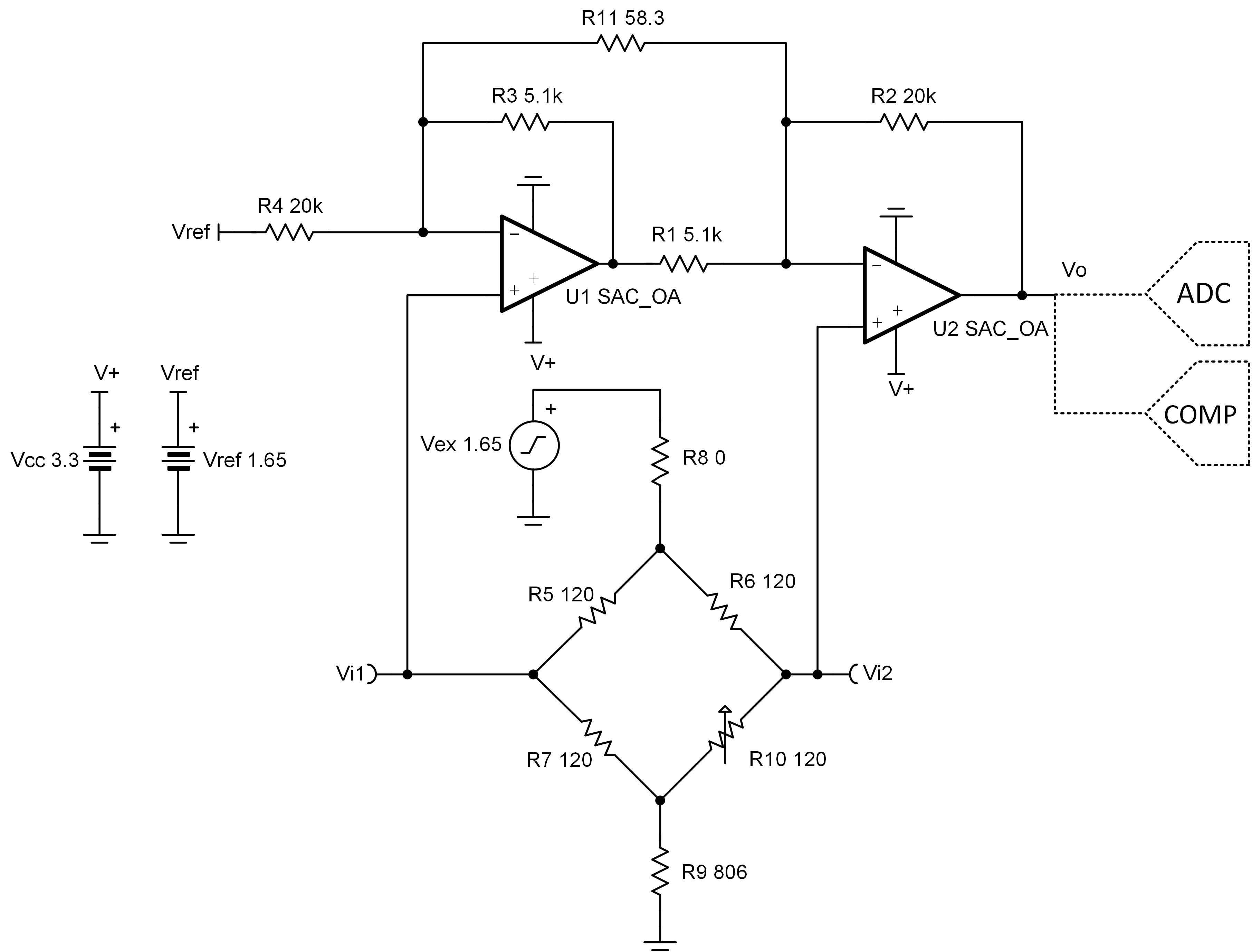
A strain gauge is a sensor whose resistance varies with applied force. The change in resistance is directly proportional to how much strain the sensor is experiencing due to the force applied. This pressure sensing circuit uses a strain gauge placed in a bridge configuration to measure the variation in resistance. This design leverages all four of the built-in op-amp blocks (SACs) in the MSP430FR2355. Two SAC_L3 peripherals are configured in general-purpose mode to amplify a differential signal created by the change in resistance of a strain gauge while the other two are configured in DAC mode to supply the reference voltage (Vref) and the excitation voltage (Vex). By varying R10, a small differential voltage is created at the output of the Wheatstone bridge which is fed to the 2 SAC op-amp instrumentation amplifier inputs. The linearity of the instrumentation amplifier is based on the input common-mode and output-swing ranges of the MSP430 SAC op-amp, which can be found in the specification chart at the end of this document. The output of the second stage op-amp can be sampled directly by the on-board ADC or monitored by the on-board comparator for further processing inside the MCU.
Design Notes
- Resistors R5, R6, and R7 of the Wheatstone bridge must match the stain gauge nominal resistance and must be equal to avoid creating a bridge offset voltage.
- Low tolerance resistors must be used to minimize the offset and gain errors due to the bridge resistors.
- Vex sets the excitation voltage of the bridge and the common-mode voltage Vcm.
- Vref biases the output voltage of the MSP430 SAC-based instrumentation amplifier to mid-supply to allow differential measurements in the positive and negative directions.
- R11 sets the gain of the instrumentation amplifier circuit.
- R8 and R9 set the common-mode voltage of the instrumentation amplifier and limits the current through the bridge. This current determines the differential signal produced by the bridge. However, there are limitations on the current through the bridge due to self-heating effects of the bridge resistors and strain gauge.
- Ensure that R1 = R3 and R2 = R4 and that ratios of R2/R1 and R4/R3 are matched to set the Vref gain to 1 V/V and maintain high DC CMRR of the instrumentation amplifier.
- Using high-value resistors can degrade the phase margin of the circuit and introduce additional noise in the circuit.
- If the solution is implemented using the MSP430FR2311, the instrumentation amplifier would need to consist of one SAC_L1 op-amp and one Transimpedance Amplifier (TIA) op-amp. The excitation and reference voltages, Vex and Vref, would need to be supplied externally (for example, voltage divider).
- The Strain Gauge Bridge Amplifier Circuit Design Files include code examples showing how to properly initialize the SAC peripherals.
Design Steps
- Select R5, R6
and R7 to match the stain gauge nominal resistance
- Choose R9 to set the
common mode voltage of the instrumentation amplifier at 1.34 V.
- Calculate the gain required to
produce the desired output voltage swing
- Select R1,
R2, R3 and R4. To set the Vref gain
at 1 V/V and avoid degrading the instrumentation amplifier’s CMRR, R1
must equal R3 and R2 equal R4.
- Calculate R11 to meet
the required gain
- Calculate
the current through the bridge
Design Simulations
DC Simulation Results
Target Applications
References
- MSP430 Strain Gauge Bridge Amplifier Circuit Code Examples and SPICE Simulation File
- Analog Engineer's Circuit Cookbooks
- MSP430FR2311 TINA-TI Spice Model
- MSP430 MCUs Smart Analog Combo Training
Design Featured Op Amp
| MSP430FRxx Smart Analog Combo | ||
|---|---|---|
| MSP430FR2311 SAC_L1 | MSP430FR2355 SAC_L3 | |
| Vcc | 2.0 V to 3.6 V | |
| VCM | -0.1 V to VCC + 0.1 V | |
| Vout | Rail-to-rail | |
| Vos | ±5 mV | |
| AOL | 100 dB | |
| Iq | 350 µA (high-speed mode) | |
| 120 µA (low-power mode) | ||
| Ib | 50 pA | |
| UGBW | 4 MHz (high-speed mode) | 2.8 MHz (high-speed mode) |
| 1.4 MHz (low-power mode) | 1 MHz (low-power mode) | |
| SR | 3 V/µs (high-speed mode) | |
| 1 V/µs (low-power mode) | ||
| Number of channels | 1 | 4 |
| MSP430FR2311 | MSP430FR2355 | |
Design Alternate Op Amp
| MSP430FR2311 Transimpedance Amplifier | |
|---|---|
| Vcc | 2.0 V to 3.6 V |
| VCM | -0.1 V to VCC/2 V |
| Vout | Rail-to-rail |
| Vos | ±5 mV |
| AOL | 100 dB |
| Iq | 350 µA (high-speed mode) |
| 120 µA (low-power mode) | |
| Ib | 5 pA (TSSOP-16 with OA-dedicated pin input) |
| 50 pA (TSSOP-20 and VQFN-16) | |
| UGBW | 5 MHz (high-speed mode) |
| 1.8 MHz (low-power mode) | |
| SR | 4 V/µs (high-speed mode) |
| 1 V/µs (low-power mode) | |
| Number of channels | 1 |
| MSP430FR2311 | |
Related MSP430 Circuits