SLAA923A November 2019 – March 2020 MSP430FR2310 , MSP430FR2311 , MSP430FR2353 , MSP430FR2355
Design Goals
| Input | Output | Supply | Full-Scale Range Error | |||
|---|---|---|---|---|---|---|
| IiMax | ViMax | VoMin | VoMax | Vcc | Vee | FSRError |
| 1 A | 250 mV | 100 mV | 2.25 V | 3.3 V | 0 V | 2.09% |
Design Description
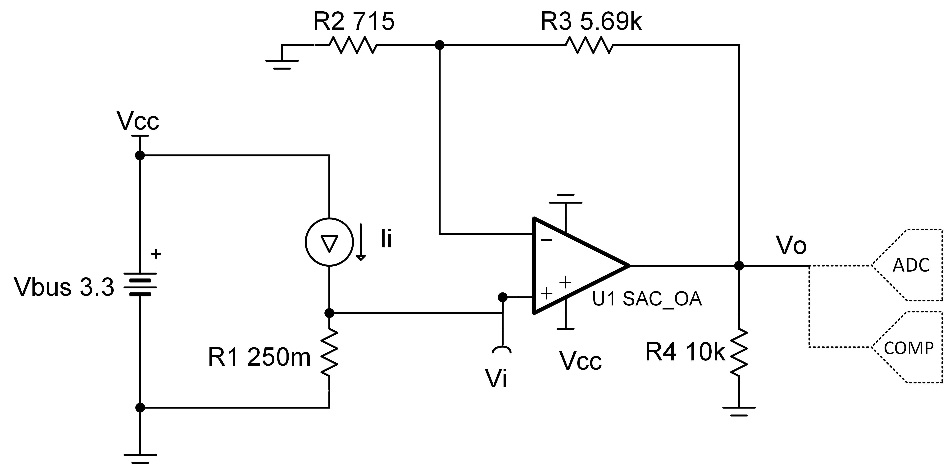
Some MSP430™ microcontrollers (MCUs) contain configurable integrated signal chain elements such as op-amps, DACs, and programmable gain stages. These elements make up a peripheral called the Smart Analog Combo (SAC). For information on the different types of SACs and how to leverage their configurable analog signal chain capabilities, visit MSP430 MCUs Smart Analog Combo Training. To get started with your design, download the Single-Supply, Low-Side, Unidirectional Current-Sensing Circuit Design Files.
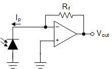
This single-supply, low-side, current sensing solution accurately detects load current up to 1 A and converts it to a voltage between 100 mV and 2.25 V. The circuit uses the MSP430FR2311 SAC_L1 op-amp in a noninverting amplifier configuration. There is room for further integration by using the programmable gain stage block within the MSP430FR2355 SAC_L3 peripheral which allows you to integrate the feedback resistor ladder (R2 and R3) into the MCU. The input current range and output voltage range can be scaled as necessary and larger supplies can be used to accommodate larger swings. The output of the second stage op-amp can be sampled directly by the onboard ADC or monitored by the onboard comparator for further processing inside the MCU.
Design Notes
- Use the op amp linear output operating range, which is usually specified under the test conditions.
- The common-mode voltage is equal to the input voltage.
- The tolerance of the shunt resistor and feedback resistors determine the gain error of the circuit.
- Avoid placing capacitive loads directly on the output of the amplifier to minimize stability issues.
- Using high-value resistors can degrade the phase margin of the circuit and introduce additional noise in the circuit.
- The small-signal bandwidth of this circuit depends on the gain of the circuit and gain bandwidth product (GBP) of the amplifier.
- Filtering can be accomplished by adding a capacitor in parallel with R3. Adding a capacitor in parallel with R3 also improves the stability of the circuit if high-value resistors are used.
- If the solution is implemented with the MSP430FR2355 SAC_L3, the op-amp can be configured in noninverting programmable gain amplifier mode or general-purpose mode with external R2 and R3 passives to measure the current-sense circuit.
- If the solution is implemented using the MSP430FR2311, the op-amp can be realized by the SAC_L1 op-amp or by the transimpedance amplifier (TIA) op-amp to measure the current-sense circuit.
- The enhanced reference module in the MSP430FR2355 can be used to scale the ADC using a VREF of 2.5 V to more accurately measure the output of the current sensing AFE.
- The Single-Supply, Low-Side, Unidirectional Current-Sensing Circuit Design Files include code examples showing how to properly initialize the SAC peripherals.
Design Steps
The transfer function for this circuit is given below.
- Define the full-scale shunt voltage and calculate the maximum shunt resistance.
- Calculate the gain required for maximum linear output voltage.
- Select standard values for R2 and R3.
- Calculate minimum input current before hitting output swing-to-rail limit. IiMin represents the minimum accurately detectable input current.
- Calculate Full scale range error and relative error. Vos is the typical offset voltage found in datasheet.
- To maintain sufficient phase margin, ensure that the zero created by the gain setting resistors and input capacitance of the device is greater than the bandwidth of the circuit
Let R2 = 715 Ω (0.1% Standard Value)
Choose R3 = 5.69 kΩ (0.1% Standard Value)
Note: The feedback resistor ladder (R2 and R3) can be realized using the integrated programmable gain resistor ladder of the SAC_L3 with a programmed noninverting gain of 9x. This implementation is showcased in the MSP430FR2355 code example. If the SAC op-amps are being used in general purpose mode, external resistors would be used to build the feedback resistor ladder.
Design Simulations
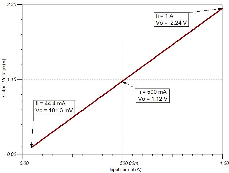
DC Simulation Results
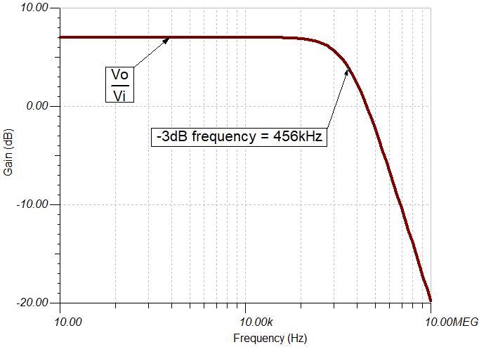
AC Simulation Results
Target Applications
- Cordless power tool battery pack
- E-bike, e-scooter battery pack
- Motor drives
- LED luminaire
- Grid infrastructure
References
- MSP430 Single-Supply, Low-Side, Unidirectional Current-Sensing Circuit Code Examples and SPICE Simulation File
- Analog Engineer's Circuit Cookbooks
- MSP430FR2311 TINA-TI Spice Model
- MSP430 MCUs Smart Analog Combo Training
Design Featured Op Amp
| MSP430FRxx Smart Analog Combo | ||
|---|---|---|
| MSP430FR2311 SAC_L1 | MSP430FR2355 SAC_L3 | |
| Vcc | 2.0 V to 3.6 V | |
| VCM | -0.1 V to VCC + 0.1 V | |
| Vout | Rail-to-rail | |
| Vos | ±5 mV | |
| AOL | 100 dB | |
| Iq | 350 µA (high-speed mode) | |
| 120 µA (low-power mode) | ||
| Ib | 50 pA | |
| UGBW | 4 MHz (high-speed mode) | 2.8 MHz (high-speed mode) |
| 1.4 MHz (low-power mode) | 1 MHz (low-power mode) | |
| SR | 3 V/µs (high-speed mode) | |
| 1 V/µs (low-power mode) | ||
| Number of channels | 1 | 4 |
| http://www.ti.com/product/MSP430FR2311 | ||
| http://www.ti.com/product/MSP430FR2355 | ||
Design Alternate Op Amp
| MSP430FR2311 Transimpedance Amplifier | |
|---|---|
| Vcc | 2.0 V to 3.6 V |
| VCM | -0.1 V to VCC/2 V |
| Vout | Rail-to-rail |
| Vos | ±5 mV |
| AOL | 100 dB |
| Iq | 350 µA (high-speed mode) |
| 120 µA (low-power mode) | |
| Ib | 5 pA (TSSOP-16 with OA-dedicated pin input) |
| 50 pA (TSSOP-20 and VQFN-16) | |
| UGBW | 5 MHz (high-speed mode) |
| 1.8 MHz (low-power mode) | |
| SR | 4 V/µs (high-speed mode) |
| 1 V/µs (low-power mode) | |
| Number of channels | 1 |
| http://www.ti.com/product/MSP430FR2311 | |
Related MSP430 Circuits