SLUAA32A October   2020  – September 2021 BQ769142 , BQ76922 , BQ76942 , BQ76952


  1.   Trademarks
  2. 1Production Programming of BQ769x2 Device Family
  3. 2Calibration
    1. 2.1 Calibration Accuracy
    2. 2.2 Cell Voltage Gain Calibration
      1. 2.2.1 Cell Voltage Gain Calibration Steps
    3. 2.3 Cell Voltage Offset Calibration
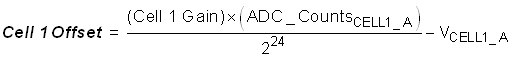
      1. 2.3.1 Cell Voltage Offset Calibration Steps
    4. 2.4 TOS (Top-of-Stack), PACK, and LD Pin Voltage Calibration
      1. 2.4.1 TOS / PACK / LD Voltage Calibration Steps
    5. 2.5 ADC Gain Calibration
    6. 2.6 Current Calibration
      1. 2.6.1 Board Offset Calibration Steps
      2. 2.6.2 CC Gain Calibration Steps
    7. 2.7 Temperature Calibration
      1. 2.7.1 Temperature Calibration Steps
    8. 2.8 COV and CUV Calibration
      1. 2.8.1 COV Calibration Steps
      2. 2.8.2 CUV Calibration Steps
    9. 2.9 Calibration Code Example
      1. 2.9.1 Code Example
      2. 2.9.2 Code Output
  4. 3OTP Programming
    1. 3.1 Recommended Steps for Writing OTP in Production
  5. 4References
  6. 5Revision History

Cell Voltage Offset Calibration Steps

  1. Calculate the offset of each cell using the meausrements taken for cell voltage gain calibration. For example, for Cell 1:
    GUID-9E2D9C88-17E3-4E73-84BB-48DB115D11F8-low.gif
  2. Calculate the average cell offset from the individual cell offsets.
  3. Write the new Cell Offset value to RAM.
    • Enter CONFIG_UPDATE mode (Subcommand 0x0090).
    • Write Cell Offset to RAM location 0x91B0.
    • Exit CONFIG UPDATE mode (Subcommand 0x0092).