SLUAA32A October 2020 – September 2021 BQ769142 , BQ76922 , BQ76942 , BQ76952
- Trademarks
- 1Production Programming of BQ769x2 Device Family
- 2Calibration
- 3OTP Programming
- 4References
- 5Revision History
2.2.1 Cell Voltage Gain Calibration Steps
The below steps are the same for each of the cells. In this example, the steps are shown for a two-point calibration of Cell 1.
- Disable Sleep Mode (Subcommand 0x009A) to ensure voltage counts update quickly after applying a voltage.
- Apply a known voltage, VCELL1_A, between device pins VC1 and VC0.
- After 100ms, read the Cell 1 Voltage Counts (ADC_CountsCELL1_A) using the DASTATUS1 subcommand 0x0071. A full list of commands for calibration voltage readings is provided in Table 2-1. For best accuracy, take multiple readings and calculate the average.
- Apply a second known voltage, VCELL1_B, between VC1 and VC0 and read the Cell 1 Voltage Counts.(ADC_CountsCELL1_B).
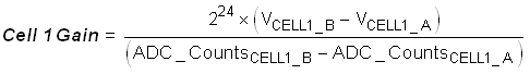
- Calculate the Cell 1 Gain:
Equation 1.
- Write the new Cell 1 Gain value to RAM.
- Enter CONFIG_UPDATE mode (Subcommand 0x0090).
- Write Cell 1 Gain to RAM location 0x9180.
- Exit CONFIG UPDATE mode (Subcommand 0x0092).
- Re-check the Cell 1 voltage reading. If the reading is not accurate, repeat steps 1-6.
Table 2-1 Voltage and Current Measurement Subcommands for Calibration
| Subcommand Address | Name | Offset | Data | Type |
|---|---|---|---|---|
| 0x0071 | DASTATUS1 | 0 | Cell 1 Voltage Counts | I4 |
| 4 | Cell 1 Current Counts | I4 | ||
| 8 | Cell 2 Voltage Counts | I4 | ||
| 12 | Cell 2 Current Counts | I4 | ||
| 16 | Cell 3 Voltage Counts | I4 | ||
| 20 | Cell 3 Current Counts | I4 | ||
| 24 | Cell 4 Voltage Counts | I4 | ||
| 28 | Cell 4 Current Counts | I4 | ||
| 0x0072 | DASTATUS2 | 0 | Cell 5 Voltage Counts | I4 |
| 4 | Cell 5 Current Counts | I4 | ||
| 8 | Cell 6 Voltage Counts | I4 | ||
| 12 | Cell 6 Current Counts | I4 | ||
| 16 | Cell 7 Voltage Counts | I4 | ||
| 20 | Cell 7 Current Counts | I4 | ||
| 24 | Cell 8 Voltage Counts | I4 | ||
| 28 | Cell 8 Current Counts | I4 | ||
| 0x0073 | DASTATUS3 | 0 | Cell 9 Voltage Counts | I4 |
| 4 | Cell 9 Current Counts | I4 | ||
| 8 | Cell 10 Voltage Counts | I4 | ||
| 12 | Cell 10 Current Counts | I4 | ||
| 16 | Cell 11 Voltage Counts | I4 | ||
| 20 | Cell 11 Current Counts | I4 | ||
| 24 | Cell 12 Voltage Counts | I4 | ||
| 28 | Cell 12 Current Counts | I4 | ||
| 0x0074 | DASTATUS4 | 0 | Cell 13 Voltage Counts | I4 |
| 4 | Cell13 Current Counts | I4 | ||
| 8 | Cell 14 Voltage Counts | I4 | ||
| 12 | Cell 14 Current Counts | I4 | ||
| 16 | Cell 15 Voltage Counts | I4 | ||
| 20 | Cell 15 Current Counts | I4 | ||
| 24 | Cell 16 Voltage Counts | I4 | ||
| 28 | Cell 16 Current Counts | I4 | ||
| 0xF081 | READ_CAL1 | 0 | Calibration Data Counter | U2 |
| 2 | CC2 Counts | I4 | ||
| 6 | PACK pin ADC Counts | I2 | ||
| 8 | Top of Stack (TOS) ADC Counts | I2 | ||
| 10 | LD pin ADC Counts | I2 |
Table 2-2 Cell Voltage Calibration Settings
| Parameter Name | Physical Start Address | Type | Min | Max | Default | Units |
|---|---|---|---|---|---|---|
| Cell 1 Gain | 0x9180 | I2 | -32767 | 32767 | 12409 | - |
| Cell 2 Gain | 0x9182 | I2 | -32767 | 32767 | 12409 | - |
| Cell 3 Gain | 0x9184 | I2 | -32767 | 32767 | 12409 | - |
| Cell 4 Gain | 0x9186 | I2 | -32767 | 32767 | 12409 | - |
| Cell 5 Gain | 0x9188 | I2 | -32767 | 32767 | 12409 | - |
| Cell 6 Gain | 0x918A | I2 | -32767 | 32767 | 12409 | - |
| Cell 7 Gain | 0x918C | I2 | -32767 | 32767 | 12409 | - |
| Cell 8 Gain | 0x918E | I2 | -32767 | 32767 | 12409 | - |
| Cell 9 Gain | 0x9190 | I2 | -32767 | 32767 | 12409 | - |
| Cell 10 Gain | 0x9192 | I2 | -32767 | 32767 | 12409 | - |
| Cell 11 Gain | 0x9194 | I2 | -32767 | 32767 | 12409 | - |
| Cell 12 Gain | 0x9196 | I2 | -32767 | 32767 | 12409 | - |
| Cell 13 Gain | 0x9198 | I2 | -32767 | 32767 | 12409 | - |
| Cell 14 Gain | 0x919A | I2 | -32767 | 32767 | 12409 | - |
| Cell 15 Gain | 0x919C | I2 | -32767 | 32767 | 12409 | - |
| Cell 16 Gain | 0x919E | I2 | -32767 | 32767 | 12409 | - |
| Vcell Offset | 0x91B0 | I2 | -32767 | 32767 | 0 | - |