SLUUBG8C November   2018  – October 2021 UCC20520 , UCC21320-Q1 , UCC21520 , UCC21520-Q1 , UCC21521 , UCC21530


  1.   Trademarks
  2. Introduction
  3. Description
  4. Features
    1. 3.1 I/O Description
    2. 3.2 Jumpers (Shunt) Setting
  5. Electrical Specifications
  6. Test Summary
    1. 5.1 Definitions
    2. 5.2 Equipment
      1. 5.2.1 Power Supplies
      2. 5.2.2 Function Generators
    3. 5.3 Equipment Setup
      1. 5.3.1 DC Power Supply Settings
      2. 5.3.2 Digital Multi-Meter Settings
      3. 5.3.3 Two-Channel Function Generator Settings
      4. 5.3.4 Oscilloscope Setting
      5. 5.3.5 Jumper (Shunt) Settings
      6. 5.3.6 Bench Setup Diagram
  7. Power-Up and Power-Down Procedure
    1. 6.1 Power Up
    2. 6.2 Power Down
  8. Test Waveforms (CL=0pF) With Different DT Configurations
    1. 7.1 DT Connected to VCCI (J-DT Option B in Table 1-1 )
    2. 7.2 DT Pin Floating or Left Open (J-DT Option A in Table 1-1 )
    3. 7.3 DT Pin Connected to RDT (J-DT Option C in Table 1-1 )
  9. Schematic
  10. Layout Diagrams
  11. 10List of Materials
  12. 11Revision History

DT Connected to VCCI (J-DT Option B in Table 3-2)

The dead time (DT) between the outputs of the two channels is decided by inputs (see Figure 7-1). Overlap between two output channels is allowed. Figure 7-1 shows a waveform with overlapped operations.
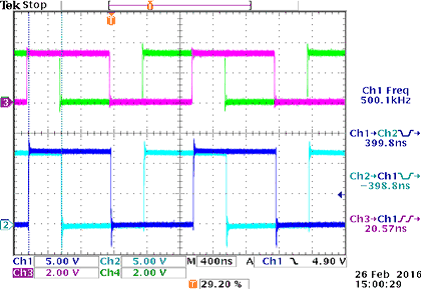
GUID-BB4AA91D-9166-45B4-9A0F-AE25EDF39124-low.gifFigure 7-1 Overlap is Allowed When DT Connected to VCCI (Channels 3 and 4 are PWM Inputs, Channels 1 and 2 are Driver Outputs)