SLVA528D September 2012 – August 2021 TPS65381-Q1 , TPS65381A-Q1
- Trademarks
- 1Introduction
- 2Product Overview
- 3Development Process for Management of Systematic Faults
- 4TPS65381x-Q1 Product Architecture for Management of Random Faults
-
5TPS65381x-Q1 Architecture Safety Mechanisms and Assumptions of Use
- 5.1 Power Supply
- 5.2 Regulated Supplies
- 5.3
Diagnostic, Monitoring, and Protection Functions
- 5.3.1 External MCU Fault Detection and Management
- 5.3.2 Voltage Monitor (VMON)
- 5.3.3 Loss-of-Clock Monitor (LCMON)
- 5.3.4 Junction Temperature Monitoring and Current Limiting
- 5.3.5 Analog and Digital MUX (AMUX and DMUX) and Diagnostic Output Pin (DIAG_OUT)
- 5.3.6 Analog Built-In Self-Test (ABIST)
- 5.3.7 Logic Built-In Self-Test (LBIST)
- 5.3.8 Device Configuration Register Protection
- 6Application Diagrams
- 7TPS65381x-Q1 as Safety Element out of Context (SEooC)
- 8Revision History
5.3.4 Junction Temperature Monitoring and Current Limiting
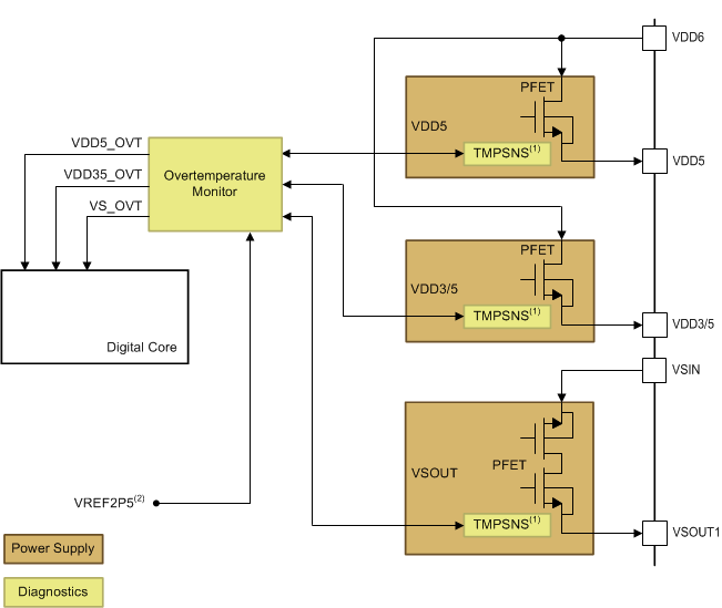
Each regulated supply with an internal power FET has junction-temperature monitoring with thermal shutdown protection. Refer to the data sheet for details on the impact of an overtemperature event on the device state and status bits for each regulator.
The VDD6, VDD3/5, VDD5, and VSOUT1 regulators include a current-limit circuit for additional protection against excessive power consumption and thermal overstress. The detection of a current limit sets a status bit for the VDD3/5 (VDD3/5_ILIM bit) and VDD5 (VDD5_ILIM bit) regulators. The current limit for the VDD3/5, VDD5, and VSOUT1 regulators may also be monitored with the diagnostic MUX output using the digital MUX (DMUX) and DIAG_OUT pin. The DMUX signal names are VDD3/5_CL, VDD5_CL and VSOUT1_CL.
The VDD6 and VDD3/5 regulators share a junction-temperature monitor, but have independent current-limiting circuits.
In a typical application, the VDD1 linear regulator controller with external FET uses VDD6 as a preregulator and receives indirect current limit from the VDD6 current limit.
