SLVA528D September 2012 – August 2021 TPS65381-Q1 , TPS65381A-Q1
- Trademarks
- 1Introduction
- 2Product Overview
- 3Development Process for Management of Systematic Faults
- 4TPS65381x-Q1 Product Architecture for Management of Random Faults
-
5TPS65381x-Q1 Architecture Safety Mechanisms and Assumptions of Use
- 5.1 Power Supply
- 5.2 Regulated Supplies
- 5.3
Diagnostic, Monitoring, and Protection Functions
- 5.3.1 External MCU Fault Detection and Management
- 5.3.2 Voltage Monitor (VMON)
- 5.3.3 Loss-of-Clock Monitor (LCMON)
- 5.3.4 Junction Temperature Monitoring and Current Limiting
- 5.3.5 Analog and Digital MUX (AMUX and DMUX) and Diagnostic Output Pin (DIAG_OUT)
- 5.3.6 Analog Built-In Self-Test (ABIST)
- 5.3.7 Logic Built-In Self-Test (LBIST)
- 5.3.8 Device Configuration Register Protection
- 6Application Diagrams
- 7TPS65381x-Q1 as Safety Element out of Context (SEooC)
- 8Revision History
5.3.2 Voltage Monitor (VMON)
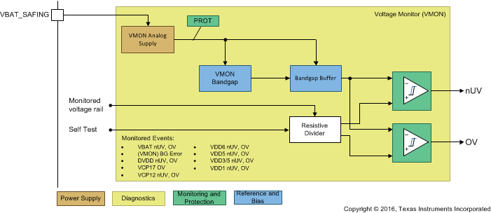
A voltage-monitor module (VMON) supervises the VBATP supply voltage, and all regulator outputs and internally generated voltages. The corresponding VMON register status flag bits indicate an undervoltage (UV) or overvoltage (OV) condition:
- VMON flag bit set to 0 when the regulator (voltage rail) is within specification
- VMON flag bit set to 1 when the regulator (voltage rail) is outside tolerance band
Undervoltage and overvoltage comparators perform the monitoring. The reference voltage (BANDGAP_REF2) for the VMON module is independent of the system reference voltage (BANDGAP_REF1) used by regulators.
A glitch-filtering function (deglitch) ensures reliable monitoring without false setting of the VMON status flag bits. A separate supply pin, VBAT_SAFING, supplies the complete VMON block.
Analog built-in self-test (ABIST) covers VMON comparator diagnostics, executed during device power up from STANDBY state. It may also be activated by the MCU though a SPI request when the device is in the DIAGNOSTIC or ACTIVE state. Emulation of each monitored voltage rail for an undervoltage and overvoltage condition on the corresponding comparator inputs forces the corresponding comparator to toggle multiple times (in a toggling pattern observed and checked by ABIST controller).
