SLVA680A February 2015 – April 2022 ESD401 , TPD12S015 , TPD12S015A , TPD12S016 , TPD12S520 , TPD12S521 , TPD13S523 , TPD1E05U06 , TPD1E10B06 , TPD1E10B09 , TPD1S414 , TPD1S514 , TPD2E001 , TPD2E001-Q1 , TPD2E009 , TPD2E1B06 , TPD2E2U06-Q1 , TPD2EUSB30 , TPD2S017 , TPD3S014 , TPD3S044 , TPD4E001-Q1 , TPD4E004 , TPD4E02B04 , TPD4E05U06 , TPD4E05U06-Q1 , TPD4E101 , TPD4E1U06 , TPD4E6B06 , TPD4EUSB30 , TPD4S010 , TPD4S014 , TPD4S1394 , TPD4S214 , TPD5S115 , TPD5S116 , TPD6E004 , TPD6E05U06 , TPD6F002-Q1 , TPD6F003 , TPD7S019 , TPD8E003 , TPD8F003
2.2 Limiting EMI from ESD
Fast transients like ESD with high di/dt can cause EMI without proper steps for suppression. For ESD, the primary source of radiation will be in the circuit between the ESD Source and the TVS. For this reason, the PCB designer should consider this region a Keep-Out area for unprotected PCB traces which could damage the system by either having direct contact with an IC, or by carrying the EMI further into the system where it could radiate more EMI. Even with no inductance at L1 (as shown in Figure 2-1) the rapidly changing electric field during ESD can couple onto nearby circuits, resulting in undesired voltages on unintended circuits. Having any induction at L1 amplifies the EMI.
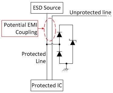
Figure 2-2 shows an unprotected line running adjacent to a protected line between the ESD Source and the TVS. This practice should be avoided. During an ESD event there will be a large dIESD/dt between the ESD Source and the TVS. The traces on this path will radiate EMI and any nearby traces could have a current induced in them by the EMI. If these traces have no TVS protecting them, the induced current in the unprotected line can cause system damage.
If there are any VIAs on the protected line between the ESD Source and the TVS, these same principles apply to any layer the VIA crosses, no unprotected lines should be ran adjacent to the VIA.
 Figure 2-2 EMI
Coupling onto an Adjacent Unprotected Trace
Figure 2-2 EMI
Coupling onto an Adjacent Unprotected TraceAnother aspect of PCB Layout to consider is the style of the corners between the ESD Source and the TVS. Corners tend to radiate EMI during IESD. The best method of routing from the ESD Source to the TVS is using straight paths which are as short as possible. Beyond lowering the impedance in the path to ground for IESD, shortening the length of this path also reduces the EMI being radiated inside the system. If corners are necessary, they should be curved with the largest radii possible, with 45° corners being the maximum angle if the PCB technology does not allow curved traces.
 Figure 2-3 Electric
Field During an 8 kV ESD Event for Three Different Corner Types
Figure 2-3 Electric
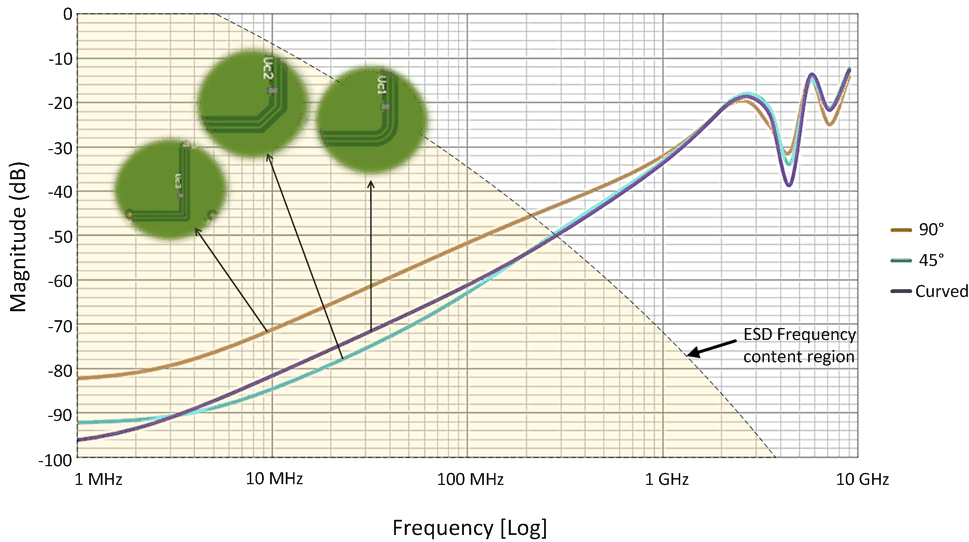
Field During an 8 kV ESD Event for Three Different Corner TypesIn Figure 2-3 note that for a 90° corner, the corner is a strong source of EMI. The electric field at the corner is at least 7 kV. This will lead to an electric arc (ionization) for any radius less than about 2.6 mm (in air). The EMI for the 45° and curve are much less pronounced. To further show the effects of corner styles, Figure 2-4 plots the crosstalk between parallel traces with these three corner types. The 90° corner has much higher coupling than the others, especially in the ESD frequency content region.
 Figure 2-4 Inter-trace Crosstalk with 45°, 90°,and Curved Corners
Summary
- Do not route unprotected circuits in the area between the ESD Source and the TVS.
- Place the TVS as near to the connector as design rules allow.
- Route with straight traces between the ESD Source and the TVS if possible.
- If corners must be used, curves are preferred and a maximum of 45° is acceptable.