SLVAED3A July 2019 – April 2024 TPS568230
5 PCB Layout
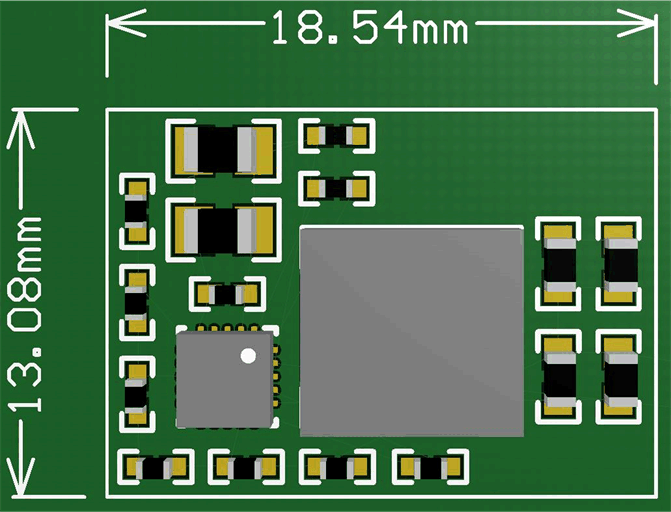
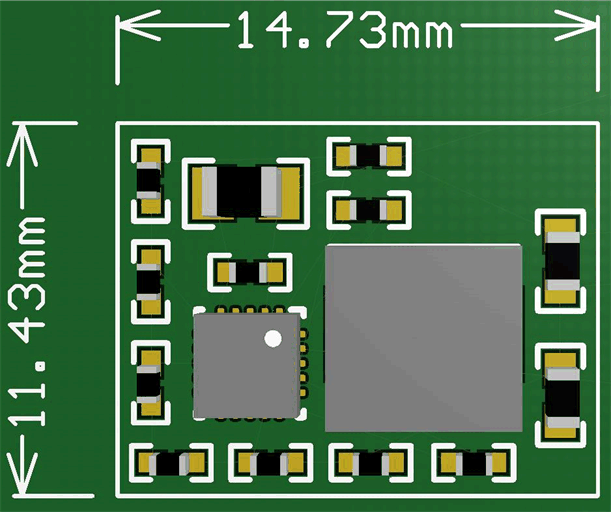
With the higher switching frequency set, the engineer can choose a smaller filter inductor and less output capacitor. Besides, a higher switching frequency is helpful for the voltage ripple of input side, so the input capacitor can also be reduced. The PCB solution size becomes smaller to achieve more flexible applications. Based on the parameters in Table 2-1, Figure 5-1 shows the PCB solution under 600 kHz. Figure 5-2 shows the PCB solution under 1000 kHz. The solution size shrinks by about 30% of 1000 kHz application compared to 600 kHz application.
 Figure 5-1 PCB
Solution, FSW = 600 kHz
 Figure 5-2 PCB
Solution, FSW = 1000 kHz