SLVAER4 August 2020 – MONTH TPS61022
2 Proposed Circuit Principle
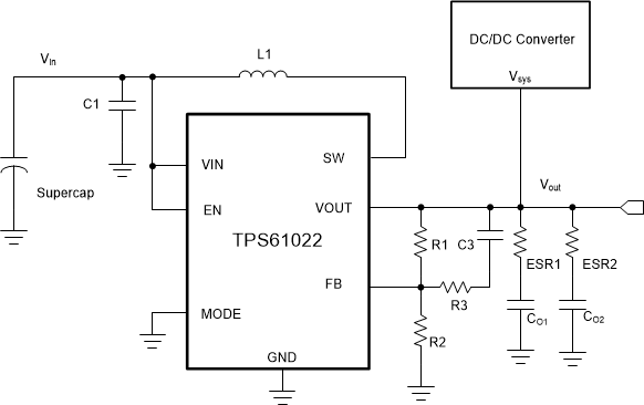
Figure 2-1 shows the theoretical circuit of the TPS61022 boost converter circuit in a supercap backup power system. The Vsys is the brief power, coming from other DC/DC converter or the grid. The TPS61022 has a MODE pin to set the operation mode. When the mode is logic high, the device operates at forced pulse width modulation (PWM) mode. At forced PWM mode, the device keeps switching with 1 MHz (VIN > 1.5 V) and 600 kHz (VIN < 1.0 V) disregarding the loading. This results in very low efficiency at light load conditions. There may be a reverse current from VOUT to charge the supercap by setting the MODE pin to logic high if the voltage of Vsys is higher than the TPS61022 setting output voltage. When the MODE is connected to a logic low voltage, the device works in auto PFM mode and there is no reverse current from VOUT to VIN by using the following configurations:
- It is recommended to connect the MODE pin to GND to set the device working at auto PFM mode. Efficiency at light load is increased and total supercap discharging time is extended.
- Set the TPS61022 VOUT 3 to 5% less than Vsys. The device does not switch when Vsys exists.
- The EN pin is connected to VIN to make the device stay in theenable state. The TPS61022 device consumes very little quiescent current (3.0 µA into VIN pin and 32 µA into the VOUT pin).
When the brief power Vsys browns out and drops less than the TPS61022 programmed output voltage VOUT, the TPS61022 starts switching and maintains VOUT at the programmed output voltage level.
 Figure 2-1 TPS61022 Boost Converter in Supercap Backup Power Applications