SLVSAC3D May 2011 – December 2014 TPS62732 , TPS62733
PRODUCTION DATA.
- 1 Features
- 2 Applications
- 3 Description
- 4 Revision History
- 5 Description (Continued)
- 6 Device Comparison Table
- 7 Pin Configuration and Functions
- 8 Specifications
- 9 Detailed Description
- 10Application and Implementation
- 11Power Supply Recommendations
- 12Layout
- 13Device and Documentation Support
- 14Mechanical, Packaging, and Orderable Information
12 Layout
12.1 Layout Guidelines
As for all switching power supplies, the layout is an important step in the design. Especially RF designs demand careful attention to the PCB layout. Care must be taken in board layout to get the specified performance. If the layout is not carefully done, the regulator could show poor line and/or load regulation, stability issues as well as EMI problems and interference with RF circuits. It is critical to provide a low inductance, impedance ground path. Therefore, use wide and short traces for the main current paths. The input capacitor should be placed as close as possible to the IC pins as well as the inductor and output capacitor. Use a common Power GND node and a different node for the Signal GND to minimize the effects of ground noise. Keep the common path to the GND PIN, which returns the small signal components and the high current of the output capacitors as short as possible to avoid ground noise. The VOUT line should be connected to the output capacitor and routed away from noisy components and traces (for example, SW line).
12.2 Layout Example
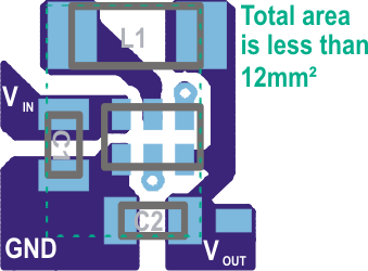 Figure 33. Recommended PCB Layout for TPS62730