SLVSAC3D May 2011 – December 2014 TPS62732 , TPS62733
PRODUCTION DATA.
- 1 Features
- 2 Applications
- 3 Description
- 4 Revision History
- 5 Description (Continued)
- 6 Device Comparison Table
- 7 Pin Configuration and Functions
- 8 Specifications
- 9 Detailed Description
- 10Application and Implementation
- 11Power Supply Recommendations
- 12Layout
- 13Device and Documentation Support
- 14Mechanical, Packaging, and Orderable Information
8 Specifications
8.1 Absolute Maximum Ratings
Over operating free-air temperature range (unless otherwise noted)(1)| MIN | MAX | UNIT | |||
|---|---|---|---|---|---|
| Voltage(2) | VIN, SW, VOUT | –0.3 | 4.2 | V | |
| ON/BYP, STAT | –0.3 | VIN + 0.3 ≤ 4.2 | V | ||
| Operating junction temperature, TJ | –40 | 125 | °C | ||
| Storage temperature, Tstg | –65 | 150 | °C | ||
(1) Stresses beyond those listed under Absolute Maximum Ratings may cause permanent damage to the device. These are stress ratings only, and functional operation of the device at these or any other conditions beyond those indicated under Recommended Operating Conditions is not implied. Exposure to absolute-maximum-rated conditions for extended periods may affect device reliability.
(2) All voltages are with respect to network ground pin.
8.2 ESD Ratings
| VALUE | UNIT | |||
|---|---|---|---|---|
| V(ESD) | Electrostatic discharge | Human body model (HBM), per ANSI/ESDA/JEDEC JS-001(1) | ±2000 | V |
| Charged-device model (CDM), per JEDEC specification JESD22-C101(2) | ±1000 | |||
| Machine model (MM), all pins | ±150 | |||
(1) JEDEC document JEP155 states that 500-V HBM allows safe manufacturing with a standard ESD control process. Manufacturing with less than 500-V HBM is possible with the necessary precautions.
(2) JEDEC document JEP157 states that 250-V CDM allows safe manufacturing with a standard ESD control process. Manufacturing with less than 250-V CDM is possible with the necessary precautions.
8.3 Recommended Operating Conditions
Operating ambient temperature TA = –40 to 85°C (unless otherwise noted)| MIN | NOM | MAX | UNIT | |||
|---|---|---|---|---|---|---|
| Supply voltage VIN | 1.9 | 3.9 | V | |||
| Effective inductance | 1.5 | 2.2 | 3 | μH | ||
| Effective output capacitance connected to VOUT | 1.0 | 10 | μF | |||
| Operating junction temperature range, TJ | –40 | 125 | °C | |||
| TA Operating free air temperature range | -40 | 85 | ||||
8.4 Thermal Information
| THERMAL METRIC(1) | TPS6273x | UNIT | |
|---|---|---|---|
| DRY | |||
| 6 PINS | |||
| θJA | Junction-to-ambient thermal resistance | 293.8 | °C/W |
| θJCtop | Junction-to-case (top) thermal resistance | 165.1 | |
| θJB | Junction-to-board thermal resistance | 160.8 | |
| ψJT | Junction-to-top characterization parameter | 27.3 | |
| ψJB | Junction-to-board characterization parameter | 159.6 | |
| θJCbot | Junction-to-case (bottom) thermal resistance | 65.8 | |
(1) For more information about traditional and new thermal metrics, see the IC Package Thermal Metrics application report, SPRA953.
8.5 Electrical Characteristics
VIN = 3.0 V, VOUT = 2.1 V, ON/BYP = VIN, TA = –40°C to 85°C typical values are at TA = 25°C (unless otherwise noted), CIN = 2.2 μF, L = 2.2 μH, COUT = 2.2 μF| PARAMETER | TEST CONDITIONS | MIN | TYP | MAX | UNIT | |||
|---|---|---|---|---|---|---|---|---|
| SUPPLY | ||||||||
| VIN | Input voltage range | 1.9 | 3.9 | V | ||||
| IQ | Operating quiescent current | ON/BYP = high, IOUT = 0mA. VIN = 3 V device not switching |
25 | 40 | μA | |||
| IOUT = 0 mA. device switching, VIN = 3.0 V, VOUT = 2.1 V | 34 | |||||||
| ON/BYP = high, Bypass switch active, VIN = VOUT = 2.1 V | 23 | |||||||
| ISD | Shutdown current, Bypass Switch Activated(2) | ON/BYP = GND, leakage current into VIN | 30 | 550 | nA | |||
| ON/BYP = GND, leakage current into VIN, TA = 60°C | 110 | |||||||
| ON/BYP | ||||||||
| VIH TH | Threshold for detecting high ON/BYP | 1.9 V ≤ VIN ≤ 3.9 V , rising edge | 0.8 | 1 | V | |||
| VIL TH | Threshold for detecting low ON/BYP | 1.9 V ≤ VIN ≤ 3.9 V , falling edge | 0.4 | 0.6 | V | |||
| IIN | Input bias Current | 0 | 50 | nA | ||||
| POWER SWITCH | ||||||||
| RDS(ON) | High side MOSFET on-resistance | VIN = 3.0 V | 600 | mΩ | ||||
| Low Side MOSFET on-resistance | 350 | |||||||
| ILIMF | Forward current limit MOSFET high side | VIN = 3.0 V, open loop | 410 | mA | ||||
| Forward current limit MOSFET low side | 410 | mA | ||||||
| BYPASS SWITCH | ||||||||
| RDS(ON) | Bypass Switch on-resistance | VIN = 2.1 V, IOUT = 20 mA, TJmax = 85°C | 2.9 | 3.8 | Ω | |||
| VIN = 3 V | 2.1 | |||||||
| VIT BYP | Automatic Bypass Switch Transition Threshold (Activation / Deactivation) | ON/BYP = high | TPS62730 (2.1 V) | ON / falling VIN | 2.14 | 2.20 | 2.3 | V |
| OFF/ rising VIN | 2.19 | 2.25 | 2.35 | |||||
| TPS62731 (2.05 V) | ON / falling VIN | 2.15 | ||||||
| OFF / rising VIN | 2.20 | |||||||
| TPS62732 (1.9 V) | ON / falling VIN | 2.05 | ||||||
| OFF / rising VIN | 2.10 | |||||||
| TPS62733 (2.3 V) | ON / falling VIN | 2.41 | ||||||
| OFF/ rising VIN | 2.48 | |||||||
| TPS62734 (2.1 V) | ON / falling VIN | 2.23 | ||||||
| OFF / rising VIN | 2.28 | |||||||
| TPS62735 (2.3 V) | ON / falling VIN | 2.23 | ||||||
| OFF / rising VIN | 2.33 | |||||||
| STAT STATUS OUTPUT (OPEN DRAIN) | ||||||||
| VTSTAT | Threshold level for STAT OUTPUT in % from VOUT | ON/BYP = high and regulator is ready, VIN falling | 95% | |||||
| ON/BYP = high and regulator is ready, VIN rising(3) | 98% | |||||||
| VOL | Output Low Voltage | Current into STAT pin I = 500 μA, VIN = 2.3 V | 0.4 | V | ||||
| VOH | Output High Voltage | Open drain output, external pull up resistor | VIN | |||||
| ILKG | Leakage into STAT pin | ON/BYP = GND, VIN = VOUT = 3 V | 0 | 50 | nA | |||
| REGULATOR | ||||||||
| tONmin | Minimum ON time | VIN = 3.0 V, VOUT = 2.1 V, IOUT = 0 mA | 180 | ns | ||||
| tOFFmin | Minimum OFF time | VIN = 2.3 V | 50 | ns | ||||
| tStart | Regulator start up time from transition ON/BYP = high to STAT = low | VIN = 3.0 V, VOUT = 3.0 V | 50 | μs | ||||
| OUTPUT | ||||||||
| VREF | Internal Reference Voltage | 0.70 | V | |||||
| VVOUT | VOUT Feedback Voltage Comparator Threshold Accuracy | VIN = 3.0 V | TA = 25°C | –1.5% | 0% | 1.5% | ||
| TA = –40°C to 85°C | –2.5% | 0% | 2.5% | |||||
| DC output voltage load regulation | IOUT = 1 mA to 50 mA VIN = 3.0 V, VOUT = 2.1 V | -0.01 | %/mA | |||||
| DC output voltage line regulation | IOUT = 20 mA, 2.4 V ≤ VIN ≤ 3.9 V | 0.01 | %/V | |||||
| ILK_SW | Leakage current into SW pin | VIN = VOUT = VSW = 3.0 V, ON/Byp= GND (1) | 0.0 | 100 | nA | |||
(1) The internal resistor divider network is disconnected from VOUT pin.
(2) Shutdown current into VIN pin, includes internal leakage
(3) The STAT output comparator is enabled once the rising input voltage exceeds the minimum input voltage VIN min of 1.9 V. In case of the 1.9 V output voltage option, the STAT output is active once the rising input voltage VIN exceeds 1.9 V.
8.6 Typical Characteristics
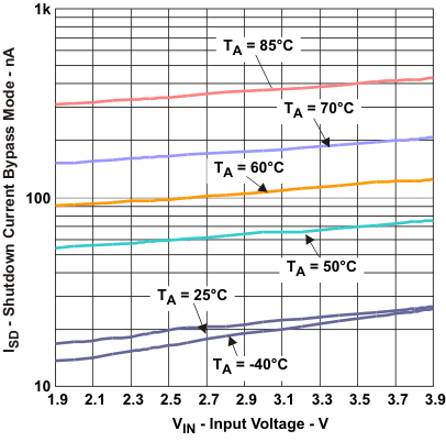 Figure 1. Shutdown Current Bypass Mode vs Input Voltage
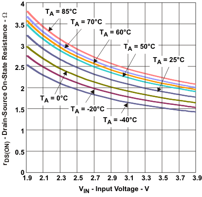 Figure 3. rDS(ON) Bypass vs Input Voltage
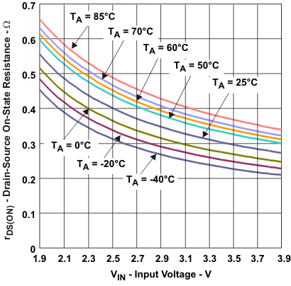 Figure 5. rDS(ON) NMOS vs Input Voltage
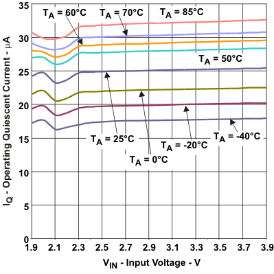 Figure 2. Operating Quiescent Current vs Input Voltage
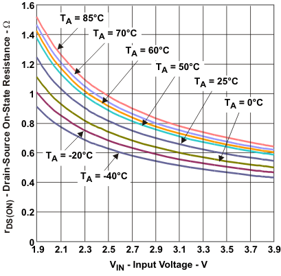 Figure 4. rDS(ON) PMOS vs Input Voltage