SLVU777A September 2012 – November 2021 TPS54020
1.3.1 Output Voltage Setpoint
The output voltage is set by the resistor divider network of R7 and R10. The lower divider resistor R10 should not be modified and should remain at 2.55 kΩ. To change the output voltage of the EVM, it is necessary to change the value of resistor R7. Changing the value of R7 changes the output voltage between 0.6 V and 5 V. The value of R7 for a specific output voltage is calculated using Equation 1.
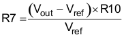
Table 1-3 lists the R7 values for some common output voltages. Note that VIN must then be within a range so that the minimum on time is greater than 150 ns. The values given in Table 1-3 show both the ideal required values and the closest E96 standard values.
| DESIRED VOUT | IDEAL R7 | CLOSEST E96 MATCH | RESULTING VOUT |
|---|---|---|---|
| 1.8 | 5.100 kΩ | 5.11 kΩ | 1.802 |
| 2.5 | 8.075 kΩ | 8.06 kΩ | 2.496 |
| 3.3 | 11.475 kΩ | 11.5 kΩ | 3.306 |
| 5.0 | 18.700 kΩ | 18.7 kΩ | 5.000 |